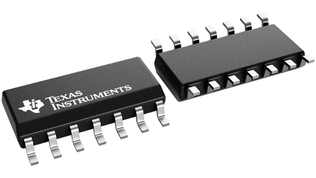
SN74AHCT126-Q1 Series
Enhanced product 4-ch, 4.5-V to 5.5-V buffers with TTL-compatible CMOS inputs and 3-state outputs
Manufacturer: Texas Instruments
Catalog
Enhanced product 4-ch, 4.5-V to 5.5-V buffers with TTL-compatible CMOS inputs and 3-state outputs
Key Features
• Controlled BaselineOne Assembly/Test Site, One Fabrication SiteExtended Temperature Performance of –40°C to 125°CEnhanced Diminishing Manufacturing Sources (DMS) SupportEnhanced Product-Change NotificationQualification PedigreeESD Protection Exceeds 2000 V Per MIL-STD-883, Method 3015; Exceeds 200 V Using Machine Model (C = 200 pF, R = 0)Inputs Are TTL-Voltage CompatibleComponent qualification in accordance with JEDEC and industry standards to ensure reliable operation over an extended temperature range. This includes, but is not limited to, Highly Accelerated Stress Test (HAST) or biased 85/85, temperature cycle, autoclave or unbiased HAST, electromigration, bond intermetallic life, and mold compound life. Such qualification testing should not be viewed as justifying use of this component beyond specified performance and environmental limits.Controlled BaselineOne Assembly/Test Site, One Fabrication SiteExtended Temperature Performance of –40°C to 125°CEnhanced Diminishing Manufacturing Sources (DMS) SupportEnhanced Product-Change NotificationQualification PedigreeESD Protection Exceeds 2000 V Per MIL-STD-883, Method 3015; Exceeds 200 V Using Machine Model (C = 200 pF, R = 0)Inputs Are TTL-Voltage CompatibleComponent qualification in accordance with JEDEC and industry standards to ensure reliable operation over an extended temperature range. This includes, but is not limited to, Highly Accelerated Stress Test (HAST) or biased 85/85, temperature cycle, autoclave or unbiased HAST, electromigration, bond intermetallic life, and mold compound life. Such qualification testing should not be viewed as justifying use of this component beyond specified performance and environmental limits.
Description
AI
The SN74AHCT126-Q1 device is a quadruple bus buffer gate featuring independent line drivers with 3-state outputs. Each output is disabled when the associated output-enable (OE) input is low. When OE is high, the respective gate passes the data from the A input to its Y output.
To ensure the high-impedance state during power up or power down, OE should be tied to GND through a pulldown resistor; the minimum value of the resistor is determined by the current-sourcing capability of the driver.


