Deep-Dive with AI
Search across all available documentation for this part.

Deep-Dive with AI
Technical Specifications
Parameters and characteristics for this part
| Specification | CD4521BM |
|---|---|
| Count Rate | 13 MHz |
| Logic Type | Divide-by-2 |
| Mounting Type | Surface Mount |
| Number of Bits per Element | 24 |
| Number of Elements | 1 |
| Operating Temperature [Max] | 125 °C |
| Operating Temperature [Min] | -55 °C |
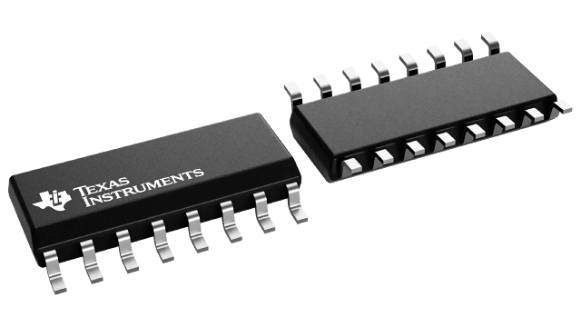
| Package / Case | 16-SOIC |
| Package / Case [x] | 0.154 in |
| Package / Case [y] | 3.9 mm |
| Reset | Asynchronous |
| Supplier Device Package | 16-SOIC |
| Trigger Type | Negative Edge |
| Voltage - Supply [Max] | 18 V |
| Voltage - Supply [Min] | 3 V |
CD4521B Series
CMOS 24-Stage Frequency Divider
| Part | Trigger Type | Voltage - Supply [Max] | Voltage - Supply [Min] | Logic Type | Number of Bits per Element | Reset | Count Rate | Package / Case | Package / Case [x] | Package / Case [y] | Supplier Device Package | Mounting Type | Number of Elements | Operating Temperature [Min] | Operating Temperature [Max] | Package / Case | Package / Case |
|---|---|---|---|---|---|---|---|---|---|---|---|---|---|---|---|---|---|
Texas Instruments | Negative Edge | 18 V | 3 V | Divide-by-2 | 24 | Asynchronous | 13 MHz | 16-SOIC | 0.154 in | 3.9 mm | 16-SOIC | Surface Mount | 1 | -55 °C | 125 °C | ||
Texas Instruments | Negative Edge | 18 V | 3 V | Divide-by-2 | 24 | Asynchronous | 13 MHz | 16-TSSOP | 0.173 in | 4.4 mm | 16-TSSOP | Surface Mount | 1 | -55 °C | 125 °C | ||
Texas Instruments | Negative Edge | 18 V | 3 V | Divide-by-2 | 24 | Asynchronous | 13 MHz | 16-TSSOP | 0.173 in | 4.4 mm | 16-TSSOP | Surface Mount | 1 | -55 °C | 125 °C | ||
Texas Instruments | Negative Edge | 18 V | 3 V | Divide-by-2 | 24 | Asynchronous | 13 MHz | 16-SOIC | 0.154 in | 3.9 mm | 16-SOIC | Surface Mount | 1 | -55 °C | 125 °C | ||
Texas Instruments | Negative Edge | 18 V | 3 V | Divide-by-2 | 24 | Asynchronous | 13 MHz | 16-SOIC | 0.154 in | 3.9 mm | 16-SOIC | Surface Mount | 1 | -55 °C | 125 °C | ||
Texas Instruments | Negative Edge | 18 V | 3 V | Divide-by-2 | 24 | Asynchronous | 13 MHz | 16-SOIC | 16-SO | Surface Mount | 1 | -55 °C | 125 °C | 0.209 " | 5.3 mm | ||
Texas Instruments | Negative Edge | 18 V | 3 V | Divide-by-2 | 24 | Asynchronous | 13 MHz | 16-SOIC | 0.154 in | 3.9 mm | 16-SOIC | Surface Mount | 1 | -55 °C | 125 °C | ||
Texas Instruments | Negative Edge | 18 V | 3 V | Divide-by-2 | 24 | Asynchronous | 13 MHz | 16-DIP | 16-PDIP | Through Hole | 1 | -55 °C | 125 °C | 0.3 in | 7.62 mm |
Pricing
Prices provided here are for design reference only. For realtime values and availability, please visit the distributors directly
| Distributor | Package | Quantity | $ | |
|---|---|---|---|---|
| Digikey | Tube | 1 | $ 1.28 | |
| 10 | $ 1.14 | |||
| 40 | $ 1.08 | |||
| 120 | $ 0.89 | |||
| 280 | $ 0.83 | |||
| 520 | $ 0.73 | |||
| Texas Instruments | TUBE | 1 | $ 0.95 | |
| 100 | $ 0.73 | |||
| 250 | $ 0.54 | |||
| 1000 | $ 0.38 | |||
Description
General part information
CD4521B Series
CD4521B consists of an oscillator section and 24 ripple-carry binary counter stages. The oscillator configuration (using IN1) allows design of either RC or crystal oscillator circuits. IN1 should be tied either HIGH or LOW when not in use. A HIGH on the RESET causes the counter to go to the all-0’s state and disables the oscillator. The count is advanced on the negative transition of IN1 (and IN2). A time-saving test mode is described in the Functional Test Sequence Table and in Fig. 6.
The CD4521B types are supplied in 16-lead dual-in-line plastic packages (E suffix), 16-lead small-outline packages (M, M96, MT, and NSR suffixes), and 16-lead thin shrink small-outline packages (PW and PWR suffixes).
CD4521B consists of an oscillator section and 24 ripple-carry binary counter stages. The oscillator configuration (using IN1) allows design of either RC or crystal oscillator circuits. IN1 should be tied either HIGH or LOW when not in use. A HIGH on the RESET causes the counter to go to the all-0’s state and disables the oscillator. The count is advanced on the negative transition of IN1 (and IN2). A time-saving test mode is described in the Functional Test Sequence Table and in Fig. 6.
Documents
Technical documentation and resources


