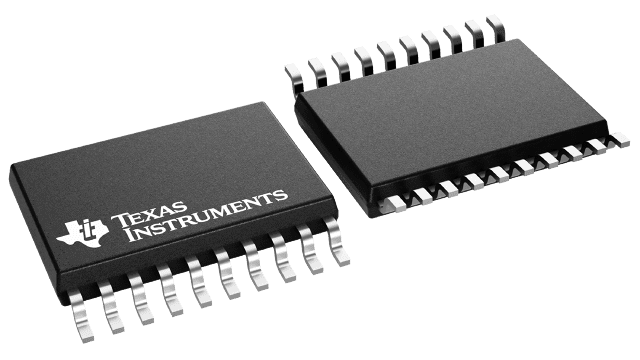
SN74LVTH273PWR
Active3.3-V ABT OCTAL D-TYPE FLIP-FLOPS WITH CLEAR
Deep-Dive with AI
Search across all available documentation for this part.

SN74LVTH273PWR
Active3.3-V ABT OCTAL D-TYPE FLIP-FLOPS WITH CLEAR
Technical Specifications
Parameters and characteristics for this part
| Specification | SN74LVTH273PWR |
|---|---|
| Clock Frequency | 150 MHz |
| Current - Output High, Low [custom] | 64 mA |
| Current - Output High, Low [custom] | 32 mA |
| Current - Quiescent (Iq) | 190 çA |
| Input Capacitance | 4 pF |
| Max Propagation Delay @ V, Max CL | 4.9 ns |
| Mounting Type | Surface Mount |
| Number of Bits per Element | 8 |
| Number of Elements | 1 |
| Operating Temperature [Max] | 85 °C |
| Operating Temperature [Min] | -40 °C |
| Output Type | Non-Inverted |
| Package / Case | 20-TSSOP |
| Package / Case [x] | 0.173 in |
| Package / Case [y] | 4.4 mm |
| Supplier Device Package | 20-TSSOP |
| Trigger Type | Positive Edge |
| Type | D-Type |
| Voltage - Supply [Max] | 3.6 V |
| Voltage - Supply [Min] | 2.7 V |
Pricing
Prices provided here are for design reference only. For realtime values and availability, please visit the distributors directly
| Distributor | Package | Quantity | $ | |
|---|---|---|---|---|
| Digikey | Cut Tape (CT) | 1 | $ 0.77 | |
| 10 | $ 0.68 | |||
| 25 | $ 0.64 | |||
| 100 | $ 0.52 | |||
| 250 | $ 0.48 | |||
| 500 | $ 0.41 | |||
| 1000 | $ 0.33 | |||
| Digi-Reel® | 1 | $ 0.77 | ||
| 10 | $ 0.68 | |||
| 25 | $ 0.64 | |||
| 100 | $ 0.52 | |||
| 250 | $ 0.48 | |||
| 500 | $ 0.41 | |||
| 1000 | $ 0.33 | |||
| Tape & Reel (TR) | 2000 | $ 0.29 | ||
| 4000 | $ 0.27 | |||
| 6000 | $ 0.26 | |||
| 10000 | $ 0.26 | |||
| Texas Instruments | LARGE T&R | 1 | $ 0.50 | |
| 100 | $ 0.39 | |||
| 250 | $ 0.28 | |||
| 1000 | $ 0.20 | |||
Description
General part information
SN74LVTH273-EP Series
These octal D-type flip-flops are designed specifically for low-voltage (3.3-V) VCCoperation, but with the capability to provide a TTL interface to a 5-V system environment.
The ’LVTH273 devices are positive-edge-triggered flip-flops with a direct-clear input. Information at the data (D) inputs meeting the setup-time requirements is transferred to the Q outputs on the positive-going edge of the clock pulse. Clock triggering occurs at a particular voltage level and is not directly related to the transition time of the positive-going pulse. When the clock (CLK) input is at either the high or low level, the D-input signal has no effect at the output.
Active bus-hold circuitry holds unused or undriven inputs at a valid logic state. Use of pullup or pulldown resistors with the bus-hold circuitry is not recommended.
Documents
Technical documentation and resources


