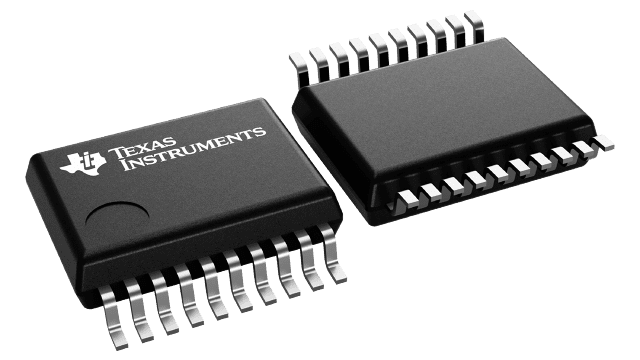
SN74LVTH273-EP Series
Enhanced Product 3.3-V Abt Octal D-Type Flip-Flops With Clear
Manufacturer: Texas Instruments
Catalog
Enhanced Product 3.3-V Abt Octal D-Type Flip-Flops With Clear
Key Features
• Controlled BaselineOne Assembly/Test Site, One Fabrication SiteEnhanced Diminishing Manufacturing Sources (DMS) SupportEnhanced Product-Change NotificationQualification PedigreeSupports Mixed-Mode Signal Operation (5-V Input and Output Voltages With 3.3-V VCC)Typical VOLP(Output Ground Bounce)<0.8 V at VCC= 3.3 V, TA= 25°CSupports Unregulated Battery Operation Down to 2.7 VBuffered Clock and Direct-Clear InputsIndividual Data Input to Each Flip-FlopIoffSupports Partial Power-Down-Mode OperationBus Hold on Data Inputs Eliminates the Need for External Pullup/Pulldown ResistorsLatch-Up Performance Exceeds 500 mA Per JESD 17ESD Protection Exceeds JESD 222000-V Human-Body Model (A114-A)200-V Machine Model (A115-A)Component qualification in accordance with JEDEC and industry standards to ensure reliable operation over an extended temperature range. This includes, but is not limited to, Highly Accelerated Stress Test (HAST) or biased 85/85, temperature cycle, autoclave or unbiased HAST, electromigration, bond intermetallic life, and mold compound life. Such qualification testing should not be viewed as justifying use of this component beyond specified performance and environmental limits.Controlled BaselineOne Assembly/Test Site, One Fabrication SiteEnhanced Diminishing Manufacturing Sources (DMS) SupportEnhanced Product-Change NotificationQualification PedigreeSupports Mixed-Mode Signal Operation (5-V Input and Output Voltages With 3.3-V VCC)Typical VOLP(Output Ground Bounce)<0.8 V at VCC= 3.3 V, TA= 25°CSupports Unregulated Battery Operation Down to 2.7 VBuffered Clock and Direct-Clear InputsIndividual Data Input to Each Flip-FlopIoffSupports Partial Power-Down-Mode OperationBus Hold on Data Inputs Eliminates the Need for External Pullup/Pulldown ResistorsLatch-Up Performance Exceeds 500 mA Per JESD 17ESD Protection Exceeds JESD 222000-V Human-Body Model (A114-A)200-V Machine Model (A115-A)Component qualification in accordance with JEDEC and industry standards to ensure reliable operation over an extended temperature range. This includes, but is not limited to, Highly Accelerated Stress Test (HAST) or biased 85/85, temperature cycle, autoclave or unbiased HAST, electromigration, bond intermetallic life, and mold compound life. Such qualification testing should not be viewed as justifying use of this component beyond specified performance and environmental limits.
Description
AI
These octal D-type flip-flops are designed specifically for low-voltage (3.3-V) VCCoperation, but with the capability to provide a TTL interface to a 5-V system environment.
The ’LVTH273 devices are positive-edge-triggered flip-flops with a direct-clear input. Information at the data (D) inputs meeting the setup-time requirements is transferred to the Q outputs on the positive-going edge of the clock pulse. Clock triggering occurs at a particular voltage level and is not directly related to the transition time of the positive-going pulse. When the clock (CLK) input is at either the high or low level, the D-input signal has no effect at the output.
Active bus-hold circuitry holds unused or undriven inputs at a valid logic state. Use of pullup or pulldown resistors with the bus-hold circuitry is not recommended.
These devices are fully specified for partial-power-down applications using Ioff. The Ioffcircuitry disables the outputs, preventing damaging current backflow through the devices when they are powered down.


