Deep-Dive with AI
Search across all available documentation for this part.

Deep-Dive with AI
Technical Specifications
Parameters and characteristics for this part
| Specification | PL133-27GC |
|---|---|
| Differential - Input:Output | False |
| Frequency - Max [Max] | 150 MHz |
| Mounting Type | Surface Mount |
| Number of Circuits | 1 |
| Operating Temperature [Max] | 70 °C |
| Operating Temperature [Min] | 0 °C |
| Output | LVCMOS |
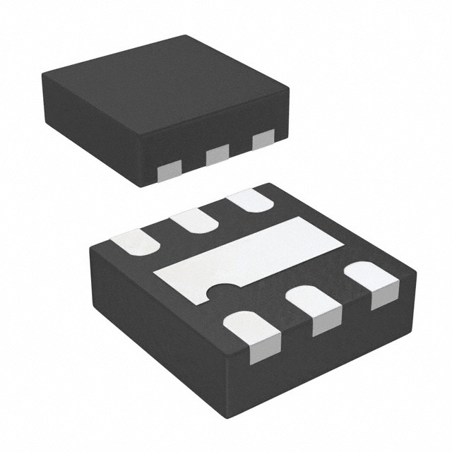
| Package / Case | 6-UFDFN Exposed Pad |
| Ratio - Input:Output [custom] | 1:2 |
| Supplier Device Package | 6-DFN (2x1.3) |
| Type | Fanout Buffer (Distribution) |
| Voltage - Supply [Max] | 3.63 V |
| Voltage - Supply [Min] | 1.62 V |
Pricing
Prices provided here are for design reference only. For realtime values and availability, please visit the distributors directly
| Distributor | Package | Quantity | $ | |
|---|---|---|---|---|
| Digikey | Bag | 1 | $ 0.97 | |
| 25 | $ 0.81 | |||
| 100 | $ 0.74 | |||
| Microchip Direct | BAG | 1 | $ 0.97 | |
| 25 | $ 0.81 | |||
| 100 | $ 0.74 | |||
| 1000 | $ 0.70 | |||
Description
General part information
PL133-47 Series
The PL133-97 is an advanced fanout buffer design for high performance, low-power, small form factor applications. The PL133-97 accepts a reference clock input from DC to 150 MHz and provides 9 outputs of the same frequency.The PL133-97 is offered in a QFN-16L 3mm x 3mm package and it offers the best phase noise, additive jitter performance, and lowest power consumption of any comparable IC. The PL133-97 outputs can be disabled to a high impedance (tri-state) by pulling low the OE pin. When the OE pin is high, the outputs are enabled and follow the REF input signal. When the OE pin is left open, a pull-up resistor on the chip will default the OE pin to logic 1 so the outputs are enabled.
Documents
Technical documentation and resources


