Deep-Dive with AI
Search across all available documentation for this part.

Deep-Dive with AI
Technical Specifications
Parameters and characteristics for this part
| Specification | SN74LVC2G132YEPR |
|---|---|
| Current - Output High, Low [x] | 32 mA |
| Current - Output High, Low [y] | 32 mA |
| Current - Quiescent (Max) [Max] | 10 µA |
| Features | Schmitt Trigger |
| Input Logic Level - High [Max] | 3.33 V |
| Input Logic Level - High [Min] | 1.16 V |
| Input Logic Level - Low [Max] | 1.87 V |
| Input Logic Level - Low [Min] | 0.39 V |
| Logic Type | NAND Gate |
| Max Propagation Delay @ V, Max CL | 5 ns |
| Mounting Type | Surface Mount |
| Number of Circuits | 2 |
| Number of Inputs | 2 |
| Operating Temperature [Max] | 85 °C |
| Operating Temperature [Min] | -40 °C |
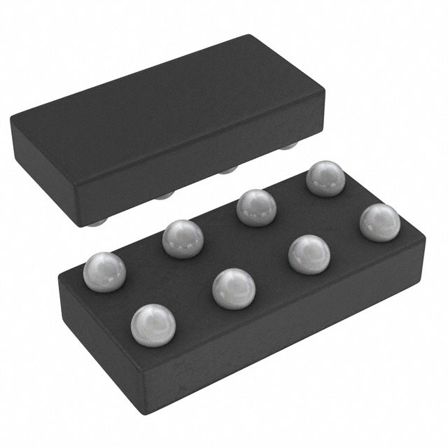
| Package / Case | 8-XFBGA, DSBGA |
| Supplier Device Package | 8-DSBGA (1.9x0.9) |
| Supplier Device Package [x] | 1.9 |
| Supplier Device Package [y] | 0.9 |
| Voltage - Supply [Max] | 5.5 V |
| Voltage - Supply [Min] | 1.65 V |
Pricing
Prices provided here are for design reference only. For realtime values and availability, please visit the distributors directly
| Distributor | Package | Quantity | $ | |
|---|---|---|---|---|
Description
General part information
SN74LVC2G132 Series
This dual 2-input NAND gate with Schmitt-trigger inputs is designed for 1.65-V to 5.5-V VCCoperation.
The SN74LVC2G132 contains two inverters and performs the Boolean function Y =A ⋅ Bor Y =A+Bin positive logic. The device functions as two independent inverters, but because of Schmitt action, it has different input threshold levels for positive-going (VT+) and negative-going (VT-) signals.
NanoFree™ package technology is a major breakthrough in IC packaging concepts, using the die as the package.
Documents
Technical documentation and resources
No documents available


