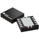
TPS51200MDRCTEP
ActiveDDR MEMORY TERMINATION REGULATOR 2.375V TO 3.5V 10-PIN VSON EP T/R
Deep-Dive with AI
Search across all available documentation for this part.

TPS51200MDRCTEP
ActiveDDR MEMORY TERMINATION REGULATOR 2.375V TO 3.5V 10-PIN VSON EP T/R
Deep-Dive with AI
Technical Specifications
Parameters and characteristics for this part
| Specification | TPS51200MDRCTEP |
|---|---|
| Applications | DDR, Converter |
| Mounting Type | Surface Mount |
| Number of Outputs | 1 |
| Operating Temperature [Max] | 125 °C |
| Operating Temperature [Min] | -55 °C |
| Package / Case | 10-VFDFN Exposed Pad |
| Supplier Device Package | 10-VSON (3x3) |
| Voltage - Input [Max] | 3.5 V |
| Voltage - Input [Min] | 2.38 V |
Pricing
Prices provided here are for design reference only. For realtime values and availability, please visit the distributors directly
| Distributor | Package | Quantity | $ | |
|---|---|---|---|---|
| Digikey | Cut Tape (CT) | 1 | $ 10.82 | |
| 10 | $ 9.94 | |||
| 25 | $ 9.53 | |||
| 100 | $ 8.40 | |||
| Digi-Reel® | 1 | $ 10.82 | ||
| 10 | $ 9.94 | |||
| 25 | $ 9.53 | |||
| 100 | $ 8.40 | |||
| Tape & Reel (TR) | 250 | $ 7.98 | ||
| 500 | $ 7.47 | |||
| 1250 | $ 6.85 | |||
| Texas Instruments | SMALL T&R | 1 | $ 9.38 | |
| 100 | $ 7.65 | |||
| 250 | $ 6.01 | |||
| 1000 | $ 5.10 | |||
Description
General part information
TPS51200A-Q1 Series
The TPS51200-Q1 device is a sink and source double-data-rate (DDR) termination regulator specifically designed for low input voltage, low-cost, low-noise systems where space is a key consideration.
The TPS51200-Q1 device maintains a fast transient response and only requires a minimum output capacitance of 20 µF. The TPS51200-Q1 device supports a remote sensing function and all power requirements for DDR, DDR2, DDR3, DDR3L, Low Power DDR3 and DDR4 VTT bus termination.
In addition, the TPS51200-Q1 device provides an open-drain PGOOD signal to monitor the output regulation and an EN signal that can be used to discharge VTT during S3 (suspend to RAM) for DDR applications.
Documents
Technical documentation and resources


