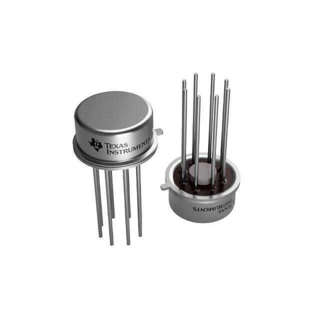
LF356 MWC
ActiveMILITARY-GRADE, SINGLE, 30-V, 5-MHZ, FET-INPUT OPERATIONAL AMPLIFIER
Deep-Dive with AI
Search across all available documentation for this part.

LF356 MWC
ActiveMILITARY-GRADE, SINGLE, 30-V, 5-MHZ, FET-INPUT OPERATIONAL AMPLIFIER
Deep-Dive with AI
Technical Specifications
Parameters and characteristics for this part
| Specification | LF356 MWC |
|---|---|
| Amplifier Type | J-FET |
| Current - Input Bias | 30 pA |
| Current - Supply | 5 mA |
| Gain Bandwidth Product | 5 MHz |
| Mounting Type | Surface Mount |
| Number of Circuits | 1 |
| Operating Temperature [Max] | 85 °C |
| Operating Temperature [Min] | -40 °C |
| Package / Case | Die |
| Slew Rate | 12 V/µs |
| Supplier Device Package | Wafersale |
| Voltage - Input Offset | 3 mV |
| Voltage - Supply Span (Max) [Max] | 36 V |
| Voltage - Supply Span (Min) [Min] | 10 V |
Pricing
Prices provided here are for design reference only. For realtime values and availability, please visit the distributors directly
| Distributor | Package | Quantity | $ | |
|---|---|---|---|---|
| Digikey | Bulk | 1701 | $ 0.45 | |
| Texas Instruments | NOT REQUIRED | 1 | $ 0.83 | |
| 100 | $ 0.64 | |||
| 250 | $ 0.47 | |||
| 1000 | $ 0.34 | |||
Description
General part information
LF356-MIL Series
The LF356-MIL device are the first monolithic JFET input operational amplifiers to incorporate well-matched, high-voltage JFETs on the same chip with standard bipolar transistors (BI-FET™ Technology). These amplifiers feature low input bias and offset currents/low offset voltage and offset voltage drift, coupled with offset adjust, which does not degrade drift or common-mode rejection. The devices are also designed for high slew rate, wide bandwidth, extremely fast settling time, low voltage and current noise and a low 1/f noise corner.
The LF356-MIL device are the first monolithic JFET input operational amplifiers to incorporate well-matched, high-voltage JFETs on the same chip with standard bipolar transistors (BI-FET™ Technology). These amplifiers feature low input bias and offset currents/low offset voltage and offset voltage drift, coupled with offset adjust, which does not degrade drift or common-mode rejection. The devices are also designed for high slew rate, wide bandwidth, extremely fast settling time, low voltage and current noise and a low 1/f noise corner.
Documents
Technical documentation and resources


