Integrated Circuits (ICs)
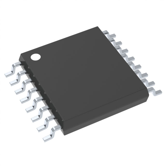
SN74LVC112APWR
ActiveTexas Instruments
DUAL NEGATIVE-EDGE-TRIGGERED J-K FLIP-FLOP WITH CLEAR AND PRESET
Deep-Dive with AI
Search across all available documentation for this part.

Integrated Circuits (ICs)
SN74LVC112APWR
ActiveTexas Instruments
DUAL NEGATIVE-EDGE-TRIGGERED J-K FLIP-FLOP WITH CLEAR AND PRESET
Technical Specifications
Parameters and characteristics for this part
| Specification | SN74LVC112APWR |
|---|---|
| Clock Frequency | 150 MHz |
| Current - Output High, Low | 24 mA |
| Current - Quiescent (Iq) | 10 µA |
| Function | Reset, Set(Preset) |
| Input Capacitance | 4.5 pF |
| Max Propagation Delay @ V, Max CL | 5.9 ns |
| Mounting Type | Surface Mount |
| Number of Bits per Element | 1 |
| Number of Elements | 2 |
| Operating Temperature [Max] | 85 °C |
| Operating Temperature [Min] | -40 °C |
| Output Type | Complementary |
| Package / Case | 16-TSSOP |
| Package / Case [x] | 0.173 in |
| Package / Case [y] | 4.4 mm |
| Supplier Device Package | 16-TSSOP |
| Trigger Type | Negative Edge |
| Type | JK Type |
| Voltage - Supply [Max] | 3.6 V |
| Voltage - Supply [Min] | 1.65 V |
Pricing
Prices provided here are for design reference only. For realtime values and availability, please visit the distributors directly
| Distributor | Package | Quantity | $ | |
|---|---|---|---|---|
| Digikey | Cut Tape (CT) | 1 | $ 0.70 | |
| 10 | $ 0.62 | |||
| 25 | $ 0.58 | |||
| 100 | $ 0.47 | |||
| 250 | $ 0.44 | |||
| 500 | $ 0.37 | |||
| 1000 | $ 0.30 | |||
| Digi-Reel® | 1 | $ 0.70 | ||
| 10 | $ 0.62 | |||
| 25 | $ 0.58 | |||
| 100 | $ 0.47 | |||
| 250 | $ 0.44 | |||
| 500 | $ 0.37 | |||
| 1000 | $ 0.30 | |||
| Tape & Reel (TR) | 2000 | $ 0.27 | ||
| 6000 | $ 0.25 | |||
| 10000 | $ 0.24 | |||
| Texas Instruments | LARGE T&R | 1 | $ 0.52 | |
| 100 | $ 0.35 | |||
| 250 | $ 0.27 | |||
| 1000 | $ 0.18 | |||
Description
General part information
SN74LVC112A Series
This dual negative-edge-triggered J-K flip-flop is designed for 1.65V to 3.6V VCC operation.
This dual negative-edge-triggered J-K flip-flop is designed for 1.65V to 3.6V VCC operation.
Documents
Technical documentation and resources


