Deep-Dive with AI
Search across all available documentation for this part.

Deep-Dive with AI
Technical Specifications
Parameters and characteristics for this part
| Specification | LMK00804BPW |
|---|---|
| Differential - Input:Output | Yes/No |
| Frequency - Max [Max] | 350 MHz |
| Input | LVDS, LVHSTL, LVCMOS, LVPECL, LVTTL, HCSL, SSTL |
| Mounting Type | Surface Mount |
| Number of Circuits | 1 |
| Operating Temperature [Max] | 85 °C |
| Operating Temperature [Min] | -40 °C |
| Output | LVCMOS, LVTTL |
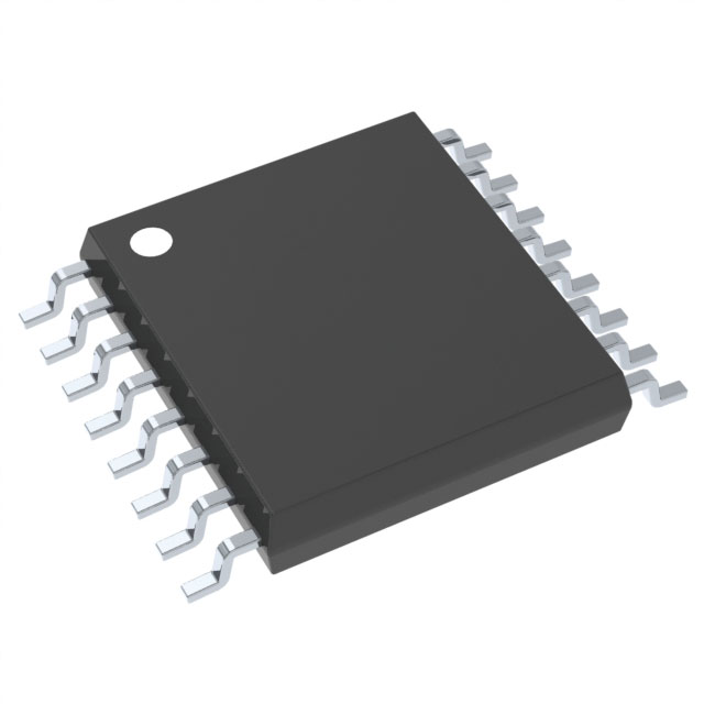
| Package / Case | 16-TSSOP |
| Package / Case [x] | 0.173 in |
| Package / Case [y] | 4.4 mm |
| Ratio - Input:Output | 1:4 |
| Supplier Device Package | 16-TSSOP |
| Type | Fanout Buffer (Distribution) |
| Voltage - Supply [Max] | 3.465 V |
| Voltage - Supply [Min] | 1.425 V |
Pricing
Prices provided here are for design reference only. For realtime values and availability, please visit the distributors directly
Description
General part information
LMK00804B-Q1 Series
The LMK00804B-Q1 is a high-performance clock fan-out buffer and level translator that can distribute up to four LVCMOS/LVTTL outputs (3.3-V, 2.5-V, 1.8-V, or 1.5-V levels) from one of two selectable inputs that can accept differential or single-ended inputs. The clock enable input is synchronized internally to eliminate runt or glitch pulses on the outputs when the clock enable terminal is asserted or deasserted. The outputs are held in logic low state when the clock is disabled. The LMK00804B-Q1 can also distribute a low-jitter clock across four transceivers and can improve the overall target detection and resolution in a cascaded mmWave radar system.
The LMK00804B-Q1 is a high-performance clock fan-out buffer and level translator that can distribute up to four LVCMOS/LVTTL outputs (3.3-V, 2.5-V, 1.8-V, or 1.5-V levels) from one of two selectable inputs that can accept differential or single-ended inputs. The clock enable input is synchronized internally to eliminate runt or glitch pulses on the outputs when the clock enable terminal is asserted or deasserted. The outputs are held in logic low state when the clock is disabled. The LMK00804B-Q1 can also distribute a low-jitter clock across four transceivers and can improve the overall target detection and resolution in a cascaded mmWave radar system.
Documents
Technical documentation and resources
No documents available


