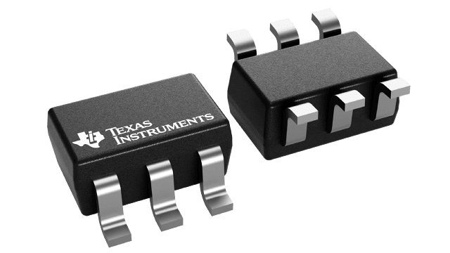
SN74LVC2G07-EP Series
Enhanced product 2-ch, 1.65-V to 5.5-V buffers with open-drain outputs
Manufacturer: Texas Instruments
Catalog
Enhanced product 2-ch, 1.65-V to 5.5-V buffers with open-drain outputs
Key Features
• Controlled BaselineOne Assembly SiteOne Test SiteOne Fabrication SiteExtended Temperature Performance of –55°C to 125°CEnhanced Diminishing Manufacturing Sources (DMS) SupportEnhanced Product-Change NotificationQualification PedigreeSupports 5-V VCCOperationInputs and Open-Drain Outputs Accept Voltages up to 5.5 VMax tpdof 5.7 ns at 3.3 VLow Power Consumption, 10 µA Max ICC±24-mA Output Drive at 3.3 VTypical VOLP(Output Ground Bounce)<0.8 V at VCC= 3.3 V, TA= 25°CTypical VOHV(Output VOHUndershoot)>2 V at VCC= 3.3 V, TA= 25°CIoffSupports Partial-Power-Down Mode OperationLatch-Up Performance Exceeds 100 mA Per JESD 78, Class IIESD Protection Exceeds JESD 222000-V Human-Body Model (A114-A)200-V Machine Model (A115-A)1000-V Charged-Device Model (C101)Component qualification in accordance with JEDEC and industry standards to ensure reliable operation over an extended temperature range. This includes, but is not limited to, Highly Accelerated Stress Test (HAST) or biased 85/85, temperature cycle, autoclave or unbiased HAST, electromigration, bond intermetallic life, and mold compound life. Such qualification testing should not be viewed as justifying use of this component beyond specified performance and environmental limits.Controlled BaselineOne Assembly SiteOne Test SiteOne Fabrication SiteExtended Temperature Performance of –55°C to 125°CEnhanced Diminishing Manufacturing Sources (DMS) SupportEnhanced Product-Change NotificationQualification PedigreeSupports 5-V VCCOperationInputs and Open-Drain Outputs Accept Voltages up to 5.5 VMax tpdof 5.7 ns at 3.3 VLow Power Consumption, 10 µA Max ICC±24-mA Output Drive at 3.3 VTypical VOLP(Output Ground Bounce)<0.8 V at VCC= 3.3 V, TA= 25°CTypical VOHV(Output VOHUndershoot)>2 V at VCC= 3.3 V, TA= 25°CIoffSupports Partial-Power-Down Mode OperationLatch-Up Performance Exceeds 100 mA Per JESD 78, Class IIESD Protection Exceeds JESD 222000-V Human-Body Model (A114-A)200-V Machine Model (A115-A)1000-V Charged-Device Model (C101)Component qualification in accordance with JEDEC and industry standards to ensure reliable operation over an extended temperature range. This includes, but is not limited to, Highly Accelerated Stress Test (HAST) or biased 85/85, temperature cycle, autoclave or unbiased HAST, electromigration, bond intermetallic life, and mold compound life. Such qualification testing should not be viewed as justifying use of this component beyond specified performance and environmental limits.
Description
AI
This dual buffer and driver is designed for 1.65-V to 5.5-V VCCoperation. The output of the SN74LVC2G07 device is open drain and can be connected to other open-drain outputs to implement active-low wired-OR or active-high wired-AND functions. The maximum sink current is 32 mA.
NanoFree package technology is a major breakthrough in IC packaging concepts, using the die as the package.
This device is fully specified for partial-power-down applications using Ioff. The Ioffcircuitry disables the outputs, preventing damaging current backflow through the device when it is powered down.


