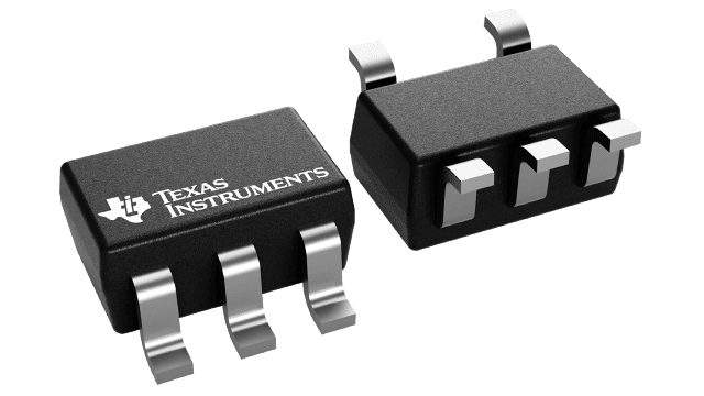
SN74AUP1G17-EP Series
Enhanced product single 0.8-V to 3.6-V low power buffer with Schmitt-Trigger inputs
Manufacturer: Texas Instruments
Catalog
Enhanced product single 0.8-V to 3.6-V low power buffer with Schmitt-Trigger inputs
Key Features
• Controlled BaselineOne Assembly/Test Site, One Fabrication SiteEnhanced Diminishing Manufacturing Sources (DMS) SupportEnhanced Product-Change NotificationQualification Pedigree(1)Available in the Texas Instruments NanoStar™ and NanoFree™ PackagesLow Static-Power Consumption (ICC= 0.9 µA Max)Low Dynamic-Power Consumption (Cpd= 4.4 pF Typ at 3.3 V)Low Input Capacitance (CI= 1.5 pF)Low Noise — Overshoot and Undershoot <10% of VCCIoffSupports Partial-Power-Down Mode OperationIncludes Schmitt-Trigger InputsWide Operating VCCRange of 0.8 V to 3.6 VOptimized for 3.3-V Operation3.6-V I/O Tolerant to Support Mixed-Mode Signal Operationtpd= 5.1 ns Max at 3.3 VSuitable for Point-to-Point ApplicationsLatch-Up Performance Exceeds 100 mA Per JESD 78, Class IIESD Performance Tested Per JESD 222000-V Human-Body Model (A114-B, Class II)200-V Machine Model (A115-A)1000-V Charged-Device Model (C101)ESD Protection Exceeds 5000 V With Human-Body Model(1)Component qualification in accordance with JEDEC and industry standards to ensure reliable operation over an extended temperature range. This includes, but is not limited to, Highly Accelerated Stress Test (HAST) or biased 85/85, temperature cycle, autoclave or unbiased HAST, electromigration, bond intermetallic life, and mold compound life. Such qualification testing should not be viewed as justifying use of this component beyond specified performance and environmental limits.NanoStar, NanoFree are trademarks of Texas Instruments.Controlled BaselineOne Assembly/Test Site, One Fabrication SiteEnhanced Diminishing Manufacturing Sources (DMS) SupportEnhanced Product-Change NotificationQualification Pedigree(1)Available in the Texas Instruments NanoStar™ and NanoFree™ PackagesLow Static-Power Consumption (ICC= 0.9 µA Max)Low Dynamic-Power Consumption (Cpd= 4.4 pF Typ at 3.3 V)Low Input Capacitance (CI= 1.5 pF)Low Noise — Overshoot and Undershoot <10% of VCCIoffSupports Partial-Power-Down Mode OperationIncludes Schmitt-Trigger InputsWide Operating VCCRange of 0.8 V to 3.6 VOptimized for 3.3-V Operation3.6-V I/O Tolerant to Support Mixed-Mode Signal Operationtpd= 5.1 ns Max at 3.3 VSuitable for Point-to-Point ApplicationsLatch-Up Performance Exceeds 100 mA Per JESD 78, Class IIESD Performance Tested Per JESD 222000-V Human-Body Model (A114-B, Class II)200-V Machine Model (A115-A)1000-V Charged-Device Model (C101)ESD Protection Exceeds 5000 V With Human-Body Model(1)Component qualification in accordance with JEDEC and industry standards to ensure reliable operation over an extended temperature range. This includes, but is not limited to, Highly Accelerated Stress Test (HAST) or biased 85/85, temperature cycle, autoclave or unbiased HAST, electromigration, bond intermetallic life, and mold compound life. Such qualification testing should not be viewed as justifying use of this component beyond specified performance and environmental limits.NanoStar, NanoFree are trademarks of Texas Instruments.
Description
AI
The AUP family of devices is TI’s premier solution to the industry’s low-power needs in battery-powered portable applications. This family ensures a very low static- and dynamic-power consumption across the entire VCCrange of 0.8 V to 3.6 V, resulting in increased battery life. This product also maintains excellent signal integrity (seeAUP – The Lowest-Power FamilyandExcellent Signal Integrity).
This device functions as an independent gate with Schmitt-trigger inputs, which allows for slow input transition and better switching-noise immunity at the input.
NanoStar™ package technology is a major breakthrough in IC packaging concepts, using the die as the package.
This device is fully specified for partial-power-down applications using Ioff. The Ioffcircuitry disables the outputs when the device is powered down. This inhibits current backflow into the device which prevents damage to the device.


