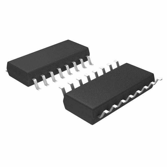
CD4502BNSR
ActiveBUFFER/DRIVER 6-CH INVERTING 3-ST CMOS 16-PIN SOP T/R
Deep-Dive with AI
Search across all available documentation for this part.

CD4502BNSR
ActiveBUFFER/DRIVER 6-CH INVERTING 3-ST CMOS 16-PIN SOP T/R
Deep-Dive with AI
Technical Specifications
Parameters and characteristics for this part
| Specification | CD4502BNSR |
|---|---|
| Current - Output High, Low [custom] | 3.4 mA |
| Current - Output High, Low [custom] | 20.4 mA |
| Logic Type | Inverting, Buffer |
| Mounting Type | Surface Mount |
| Number of Bits per Element | 6 |
| Number of Elements | 1 |
| Operating Temperature [Max] | 125 °C |
| Operating Temperature [Min] | -55 °C |
| Output Type | Push-Pull |
| Package / Case | 0.209 " |
| Package / Case | 16-SOIC |
| Package / Case | 5.3 mm |
| Supplier Device Package | 16-SO |
| Voltage - Supply [Max] | 18 V |
| Voltage - Supply [Min] | 3 V |
Pricing
Prices provided here are for design reference only. For realtime values and availability, please visit the distributors directly
| Distributor | Package | Quantity | $ | |
|---|---|---|---|---|
| Digikey | Cut Tape (CT) | 1 | $ 1.57 | |
| 10 | $ 0.99 | |||
| 25 | $ 0.84 | |||
| 100 | $ 0.67 | |||
| 250 | $ 0.58 | |||
| 500 | $ 0.53 | |||
| 1000 | $ 0.49 | |||
| Digi-Reel® | 1 | $ 1.57 | ||
| 10 | $ 0.99 | |||
| 25 | $ 0.84 | |||
| 100 | $ 0.67 | |||
| 250 | $ 0.58 | |||
| 500 | $ 0.53 | |||
| 1000 | $ 0.49 | |||
| Tape & Reel (TR) | 2000 | $ 0.35 | ||
| 4000 | $ 0.33 | |||
| 6000 | $ 0.31 | |||
| 10000 | $ 0.30 | |||
| 14000 | $ 0.29 | |||
| 20000 | $ 0.28 | |||
| Texas Instruments | LARGE T&R | 1 | $ 0.94 | |
| 100 | $ 0.64 | |||
| 250 | $ 0.49 | |||
| 1000 | $ 0.33 | |||
Description
General part information
CD4502B Series
CD4502B consists of six inverter/buffers with 3-state outputs. A logic "1" on the OUTPUT DISABLE input produces a high-impedance state in all six outputs. This feature permits common busing of the outputs, thus simplifying system design. A Logic "1" on the INHIBIT input switches all six outputs to logic "0" if the OUTPUT DISABLE input is a logic "0". This device is capable of driving two standard TTL loads, which is equivalent to six times the JEDEC "B"-series IOLstandard.
The CD4502B types are supplied in 16-lead hermetic dual-in-line ceramic packages (F3A suffix), 16-lead dual-in-line plastic packages (E suffix), 16-lead small-outline packages (NSR suffix), and 16-lead thin shrink small-outline packages (PW and PWR suffixes).
CD4502B consists of six inverter/buffers with 3-state outputs. A logic "1" on the OUTPUT DISABLE input produces a high-impedance state in all six outputs. This feature permits common busing of the outputs, thus simplifying system design. A Logic "1" on the INHIBIT input switches all six outputs to logic "0" if the OUTPUT DISABLE input is a logic "0". This device is capable of driving two standard TTL loads, which is equivalent to six times the JEDEC "B"-series IOLstandard.
Documents
Technical documentation and resources


