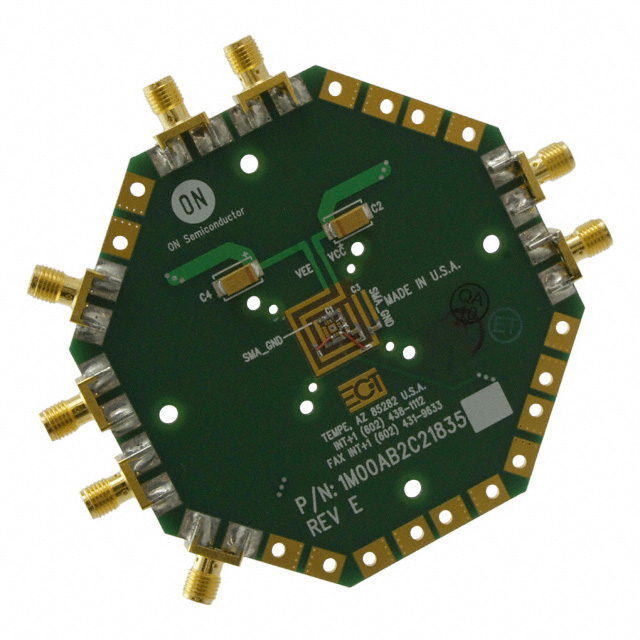
NB4N527SMNEVB
ActiveEVALUATION BOARD, NB4N527S TRANSLATOR, ANYLEVEL TO LVDS, 1.25GHZ, 2.5GB/S, INTERNAL TERMINATION
Deep-Dive with AI
Search across all available documentation for this part.

NB4N527SMNEVB
ActiveEVALUATION BOARD, NB4N527S TRANSLATOR, ANYLEVEL TO LVDS, 1.25GHZ, 2.5GB/S, INTERNAL TERMINATION
Deep-Dive with AI
Technical Specifications
Parameters and characteristics for this part
| Specification | NB4N527SMNEVB |
|---|---|
| Contents | Board(s) |
| Embedded | False |
| Function | Clock Buffer, Translator, Driver, Receiver |
| Primary Attributes | Four Layer Board with Split (Dual) Power Supplies |
| Secondary Attributes | SMA Connectors |
| Type | Timing |
| Utilized IC / Part | NB4N527S |
Pricing
Prices provided here are for design reference only. For realtime values and availability, please visit the distributors directly
Description
General part information
NB4N527S Series
NB4N527S is a clock or data Receiver/Driver/Buffer/Translator capable of translating AnyLevelTMinput signal (LVPECL, CML, HSTL, LVDS, or LVTTL/LVCMOS) to LVDS. Depending on the distance, noise immunity of the system design, and transmission line media, this device will receive, drive or translate data or clock signals up to 2.5 Gb/s or 1.25 GHz, respectively.The NB4N527S has a wide input common mode range of GND+50 mV to VCC-50 mV combined with two 50 Ω internal termination resistors is ideal for translating differential or single-ended data or clock signals to 350 mV typical LVDS output levels without use of any additional external components.The device is offered in a small 3 mm x 3 mm QFN-16 package. NB4N527S is targeted for data, wireless and telecom applications as well as high speed logic interface where jitter and package size are main requirements.
Documents
Technical documentation and resources


