Deep-Dive with AI
Search across all available documentation for this part.

Deep-Dive with AI
Technical Specifications
Parameters and characteristics for this part
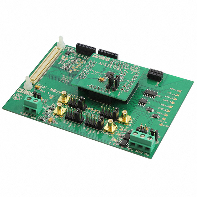
| Specification | EVAL-AD5323DBZ |
|---|---|
| DAC Type | Voltage |
| Data Interface | SPI, Serial |
| Number of Bits | 12 bits |
| Number of DAC's | 2 |
| Settling Time | 8 µs |
| Supplied Contents | Board(s) |
| Utilized IC / Part | AD5323 |
Pricing
Prices provided here are for design reference only. For realtime values and availability, please visit the distributors directly
| Distributor | Package | Quantity | $ | |
|---|---|---|---|---|
| Digikey | Bulk | 1 | $ 79.09 | |
Description
General part information
AD5323 Series
TheAD5303/AD5313/ AD5323 are dual 8-/10-/12-bit buffered voltage output DACs in a 16-lead TSSOP package that operate from a single 2.5 V to 5.5 V supply, consuming 230 μA at 3 V. Their on-chip output amplifiers allow the outputs to swing rail-to-rail with a slew rate of 0.7 V/μs. The AD5313 / AD5323 utilize a versatile 3-wire serial interface that operates at clock rates up to 30 MHz and is compatible with standard SPI, QSPI™, MICROWIRE™, and DSP interface standardsThe references for the two DACs are derived from two reference pins (one per DAC). These reference inputs may be configured as buffered or unbuffered inputs. The parts incorporate a power-on reset circuit, which ensures that the DAC outputs power up to 0 V and remain there until a valid write to the device takes place. There is also an asynchronous active low CLR pin that clears both DACs to 0 V. The outputs of both DACs may be updated simultaneously using the asynchronous LDAC input. The parts contain a power-down feature that reduces the current consumption of the devices to 200 nA at 5 V (50 nA at 3 V) and provides software-selectable output loads while in power-down mode. The parts may also be used in daisy-chaining applications using the SDO pin.The low power consumption of these parts in normal operation makes them ideally suited to portable battery-operated equipment. The power consumption is 1.5 mW at 5 V and 0.7 mW at 3 V, reducing to 1 μW in power-down mode.APPLICATIONSPortable battery-powered instrumentsDigital gain and offset adjustmentProgrammable voltage and current sourcesProgrammable attenuators
Documents
Technical documentation and resources


