Deep-Dive with AI
Search across all available documentation for this part.

Deep-Dive with AI
Technical Specifications
Parameters and characteristics for this part
| Specification | TPS61170DRVRG4 |
|---|---|
| Current - Output | 960 mA |
| Frequency - Switching | 1.2 MHz |
| Function | Step-Up/Step-Down, Step-Up |
| Mounting Type | Surface Mount |
| Number of Outputs | 1 |
| Operating Temperature [Max] | 85 C |
| Operating Temperature [Min] | -40 ¯C |
| Output Configuration | Positive |
| Output Type | Adjustable |
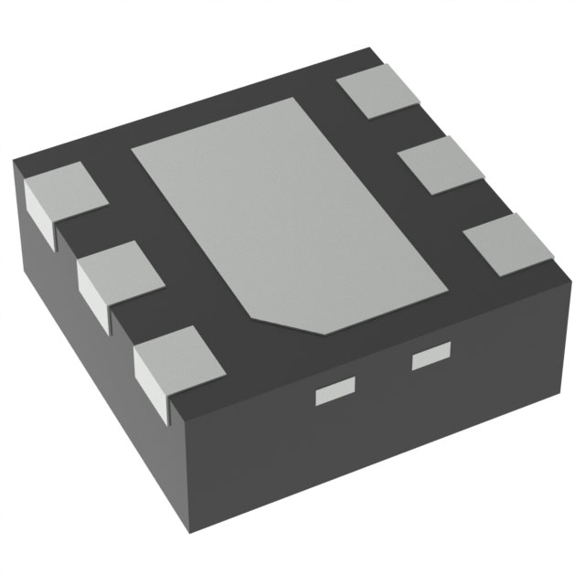
| Supplier Device Package | 6-WSON (2x2) |
| Synchronous Rectifier | False |
| Topology | Flyback, Boost, SEPIC, Buck-Boost |
| Voltage - Input (Max) [Max] | 18 V |
| Voltage - Input (Min) [Min] | 3 V |
| Voltage - Output (Max) [Max] | 38 V |
| Voltage - Output (Min/Fixed) | 3 V |
Pricing
Prices provided here are for design reference only. For realtime values and availability, please visit the distributors directly
| Distributor | Package | Quantity | $ | |
|---|---|---|---|---|
| Digikey | Cut Tape (CT) | 1 | $ 1.17 | |
| Digi-Reel® | 1 | $ 1.17 | ||
| N/A | 0 | $ 1.04 | ||
| Tape & Reel (TR) | 3000 | $ 0.49 | ||
| 6000 | $ 0.47 | |||
| 15000 | $ 0.45 | |||
Description
General part information
TPS61170 Series
The TPS61170-Q1 is a monolithic, high-voltage switching regulator with integrated 1.2-A, 40-V power MOSFET. The device can be configured in several standard switching-regulator topologies, including boost and SEPIC. The device has a wide input-voltage range to support applications with input voltage from multicell batteries or regulated 5-V, 12-V power rails.
The TPS61170-Q1 operates at a 1.2-MHz switching frequency, allowing the use of low-profile inductors and low-value ceramic input and output capacitors. External loop compensation components give the user flexibility to optimize loop compensation and transient response. The device has built-in protection features, such as pulse-by-pulse overcurrent limit, soft start, and thermal shutdown.
The FB pin regulates to a reference voltage of1.229 V. The reference voltage can be lowered using a 1-wire digital interface (EasyScale™ protocol) through the CTRL pin. Alternatively, a pulse width-modulation (PWM) signal can be applied to the CTRL pin. The duty cycle of the signal reduces the feedback reference voltage proportionally.
Documents
Technical documentation and resources
No documents available


