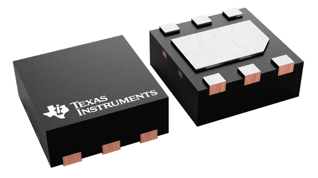
TPS61170DRVR
Active1.2A SWITCH, 38V HIGH VOLTAGE BOOST CONVERTER IN 2X2MM QFN PACKAGE
Deep-Dive with AI
Search across all available documentation for this part.

TPS61170DRVR
Active1.2A SWITCH, 38V HIGH VOLTAGE BOOST CONVERTER IN 2X2MM QFN PACKAGE
Technical Specifications
Parameters and characteristics for this part
| Specification | TPS61170DRVR |
|---|---|
| Current - Output | 960 mA |
| Frequency - Switching | 1.2 MHz |
| Function | Step-Up/Step-Down, Step-Up |
| Mounting Type | Surface Mount |
| Number of Outputs | 1 |
| Operating Temperature [Max] | 85 C |
| Operating Temperature [Min] | -40 ¯C |
| Output Configuration | Positive |
| Output Type | Adjustable |
| Supplier Device Package | 6-WSON (2x2) |
| Synchronous Rectifier | False |
| Topology | Flyback, Boost, SEPIC, Buck-Boost |
| Voltage - Input (Max) [Max] | 18 V |
| Voltage - Input (Min) [Min] | 3 V |
| Voltage - Output (Max) [Max] | 38 V |
| Voltage - Output (Min/Fixed) | 3 V |
TPS61170 Series
3-V to 18-V wide input range, 1.2-A boost converter in 2-mm x 2-mm QFN package, AEC-Q100 qualified
| Part | Output Type | Supplier Device Package | Voltage - Output (Max) [Max] | Voltage - Input (Max) [Max] | Voltage - Input (Min) [Min] | Frequency - Switching | Output Configuration | Topology | Mounting Type | Number of Outputs | Synchronous Rectifier | Operating Temperature [Max] | Operating Temperature [Min] | Current - Output | Function | Voltage - Output (Min/Fixed) | Board Type | Supplied Contents | Outputs and Type | Outputs and Type | Utilized IC / Part | Contents | Voltage - Input [Max] | Voltage - Input [Min] | Main Purpose | Voltage - Output | Regulator Topology | Qualification | Grade |
|---|---|---|---|---|---|---|---|---|---|---|---|---|---|---|---|---|---|---|---|---|---|---|---|---|---|---|---|---|---|
Texas Instruments | Adjustable | 6-WSON (2x2) | 38 V | 18 V | 3 V | 1.2 MHz | Positive | Boost Buck-Boost Flyback SEPIC | Surface Mount | 1 | 85 C | -40 ¯C | 960 mA | Step-Up Step-Up/Step-Down | 3 V | ||||||||||||||
Texas Instruments | 1.2 MHz | 420 mA | Fully Populated | Board(s) | 1 | 1 Non-Isolated Output Non-Isolated | TPS61170 | Board(s) | 15 V | 9 V | DC/DC Step Up or Down | 12 V | Buck-Boost | ||||||||||||||||
Texas Instruments | Adjustable | 6-WSON (2x2) | 38 V | 18 V | 3 V | 1.2 MHz | Positive | Boost Buck-Boost Flyback SEPIC | Surface Mount | 1 | 85 C | -40 ¯C | 960 mA | Step-Up Step-Up/Step-Down | 3 V | ||||||||||||||
Texas Instruments | Adjustable | 6-WSON (2x2) | 38 V | 18 V | 3 V | 1.2 MHz | Positive | Boost Buck-Boost Flyback SEPIC | Surface Mount | 1 | 85 C | -40 ¯C | 960 mA | Step-Up Step-Up/Step-Down | 3 V | ||||||||||||||
Texas Instruments | 1.2 MHz | 550 mA | Fully Populated | Board(s) | 1 | 1 Non-Isolated Output Non-Isolated | TPS61170 | Board(s) | 18 V | 9 V | DC/DC Step Up | 24 V | Boost | ||||||||||||||||
Texas Instruments | Adjustable | 6-WSON (2x2) | 38 V | 18 V | 3 V | 1.2 MHz | Positive | Boost Buck-Boost Flyback SEPIC | Surface Mount | 1 | 125 °C | -40 °C | 960 mA | Step-Up Step-Up/Step-Down | 3 V | AEC-Q100 | Automotive |
Pricing
Prices provided here are for design reference only. For realtime values and availability, please visit the distributors directly
| Distributor | Package | Quantity | $ | |
|---|---|---|---|---|
| Digikey | N/A | 8214 | $ 2.19 | |
| Texas Instruments | LARGE T&R | 1 | $ 1.61 | |
| 100 | $ 1.24 | |||
| 250 | $ 0.91 | |||
| 1000 | $ 0.65 | |||
Description
General part information
TPS61170 Series
The TPS61170-Q1 is a monolithic, high-voltage switching regulator with integrated 1.2-A, 40-V power MOSFET. The device can be configured in several standard switching-regulator topologies, including boost and SEPIC. The device has a wide input-voltage range to support applications with input voltage from multicell batteries or regulated 5-V, 12-V power rails.
The TPS61170-Q1 operates at a 1.2-MHz switching frequency, allowing the use of low-profile inductors and low-value ceramic input and output capacitors. External loop compensation components give the user flexibility to optimize loop compensation and transient response. The device has built-in protection features, such as pulse-by-pulse overcurrent limit, soft start, and thermal shutdown.
The FB pin regulates to a reference voltage of1.229 V. The reference voltage can be lowered using a 1-wire digital interface (EasyScale™ protocol) through the CTRL pin. Alternatively, a pulse width-modulation (PWM) signal can be applied to the CTRL pin. The duty cycle of the signal reduces the feedback reference voltage proportionally.
Documents
Technical documentation and resources


