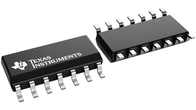
SN74LVC00AD
Active4-CH, 2-INPUT, 1.65-V TO 3.6-V NAND GATES
Deep-Dive with AI
Search across all available documentation for this part.

SN74LVC00AD
Active4-CH, 2-INPUT, 1.65-V TO 3.6-V NAND GATES
Technical Specifications
Parameters and characteristics for this part
| Specification | SN74LVC00AD |
|---|---|
| Current - Output High, Low | 24 mA |
| Current - Quiescent (Max) [Max] | 1 çA |
| Input Logic Level - High [Max] | 2 V |
| Input Logic Level - High [Min] | 1.7 V |
| Input Logic Level - Low [Max] | 0.8 V |
| Input Logic Level - Low [Min] | 0.7 V |
| Logic Type | NAND Gate |
| Max Propagation Delay @ V, Max CL | 4.1 ns |
| Mounting Type | Surface Mount |
| Number of Circuits | 4 |
| Number of Inputs | 2 |
| Operating Temperature [Max] | 125 °C |
| Operating Temperature [Min] | -40 °C |
| Package / Case | 14-SOIC |
| Package / Case [x] | 0.154 in |
| Package / Case [y] | 3.9 mm |
| Voltage - Supply [Max] | 3.6 V |
| Voltage - Supply [Min] | 1.65 V |
Pricing
Prices provided here are for design reference only. For realtime values and availability, please visit the distributors directly
| Distributor | Package | Quantity | $ | |
|---|---|---|---|---|
| Digikey | Tube | 1 | $ 1.02 | |
| 10 | $ 0.91 | |||
| 50 | $ 0.86 | |||
| 100 | $ 0.71 | |||
| 250 | $ 0.66 | |||
| 500 | $ 0.59 | |||
| 1000 | $ 0.46 | |||
| 2500 | $ 0.43 | |||
| 5000 | $ 0.41 | |||
| Texas Instruments | TUBE | 1 | $ 0.88 | |
| 100 | $ 0.59 | |||
| 250 | $ 0.46 | |||
| 1000 | $ 0.30 | |||
Description
General part information
SN74LVC00A-EP Series
The SN54LVC00A quadruple 2-input positive-NAND gate is designed for 2.7V to 3.6V VCC operation, and the SN74LVC00A quadruple 2-input positive-NAND gate is designed for 1.65V to 3.6V VCC operation.
The SNx4LVC00A devices perform the Boolean function Y = A • B or Y = A + B in positive logic.
Inputs can be driven from either 3.3V or 5V devices. This feature allows the use of these devices as translators in a mixed 3.3V/5V system environment.
Documents
Technical documentation and resources


