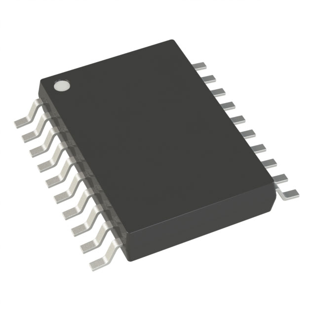
AD5791SRUZ-EP
Active1 PPM, 20-BIT, ±1 LSB INL, VOLTAGE OUTPUT DAC
Deep-Dive with AI
Search across all available documentation for this part.

AD5791SRUZ-EP
Active1 PPM, 20-BIT, ±1 LSB INL, VOLTAGE OUTPUT DAC
Deep-Dive with AI
Technical Specifications
Parameters and characteristics for this part
| Specification | AD5791SRUZ-EP |
|---|---|
| Data Interface | Serial |
| Differential Output | True |
| INL/DNL (LSB) | ±1 (Max) |
| Mounting Type | Surface Mount |
| Number of Bits | 20 |
| Operating Temperature [Max] | 125 °C |
| Operating Temperature [Min] | -55 °C |
| Output Type | Voltage - Unbuffered |
| Package / Case | 20-TSSOP |
| Package / Case [x] | 0.173 in |
| Package / Case [y] | 4.4 mm |
| Reference Type | External |
| Settling Time | 1 µs |
| Supplier Device Package | 20-TSSOP |
| Voltage - Supply, Analog [Max] | 5.5 V |
| Voltage - Supply, Analog [Min] | 2.7 V |
| Voltage - Supply, Digital [Max] | 5.5 V |
| Voltage - Supply, Digital [Min] | 2.7 V |
Pricing
Prices provided here are for design reference only. For realtime values and availability, please visit the distributors directly
| Distributor | Package | Quantity | $ | |
|---|---|---|---|---|
| Digikey | Tube | 1 | $ 271.21 | |
Description
General part information
AD5791 Series
The AD57911is a single 20-bit, unbuffered voltage-output DAC that operates from a bipolar supply of up to 33 V. The AD5791 accepts a positive reference input in the range 5 V to VDD– 2.5 V and a negative reference input in the range VSS+ 2.5 V to 0 V. The AD5791 offers a relative accuracy specification of ±1 LSB max, and operation is guaranteed monotonic with a ±1 LSB differential nonlinearity (DNL) maximum specification.The device uses a versatile 3-wire serial interface that operates at clock rates up to 35 MHz and that is compatible with standard serial peripheral interface (SPI), QSPI™, MICROWIRE™, and DSP interface standards. The device incorporates a power-on reset circuit that ensures the DAC output powers up to 0 V and in a known output impedance state and remains in this state until a valid write to the device takes place. The device provides an output clamp feature that places the output in a defined load state.Product Highlights1 ppm Accuracy.Wide Power Supply Range up to ±16.5 V.Operating Temperature Range: −40°C to +125°C.Low 7.5 nV/√Hz Noise Spectral Density.Low 0.05 ppm/°C Temperature Drift.ApplicationsMedical instrumentationTest and measurementIndustrial controlHigh end scientific and aerospace instrumentation1Protected by U.S. Patent No. 7,884,747. Other patents pending.
Documents
Technical documentation and resources


