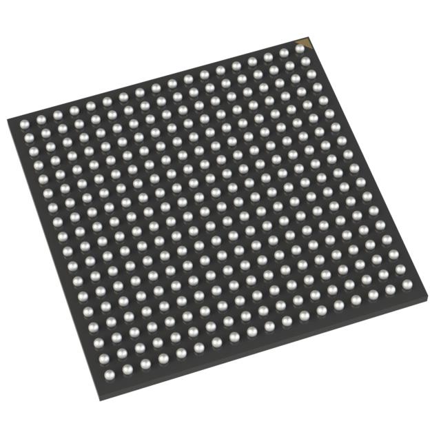
AD9207BBPZ-6G
Active12-BIT, 6 GSPS, JESD204B/JESD204C DUAL ADC
Deep-Dive with AI
Search across all available documentation for this part.

AD9207BBPZ-6G
Active12-BIT, 6 GSPS, JESD204B/JESD204C DUAL ADC
Deep-Dive with AI
Technical Specifications
Parameters and characteristics for this part
| Specification | AD9207BBPZ-6G |
|---|---|
| Configuration | MUX-ADC |
| Data Interface | JESD204B/C |
| Features | Temperature Sensor |
| Input Type | Differential |
| Mounting Type | Surface Mount |
| Number of A/D Converters | 2 |
| Number of Bits | 12 bits |
| Number of Inputs | 2 |
| Operating Temperature [Max] | 120 °C |
| Operating Temperature [Min] | -40 °C |
| Package / Case | 324-FBGA Exposed Pad |
| Ratio - S/H:ADC | 1:1 |
| Sampling Rate (Per Second) | 6 G |
| Supplier Device Package | 324-BGA-ED (15x15) |
Pricing
Prices provided here are for design reference only. For realtime values and availability, please visit the distributors directly
| Distributor | Package | Quantity | $ | |
|---|---|---|---|---|
| Digikey | Tray | 1 | $ 1323.10 | |
Description
General part information
AD9207 Series
The AD9207 is a dual, 12-bit, 6 GSPS analog-to-digital converter (ADC). The ADC input features an on-chip wideband buffer with overload protection. This device is designed to support applications capable of direct sampling wideband signals up to 8 GHz. An onchip, low phase noise, phase-locked loop (PLL) clock synthesizer is available to generate the ADC sampling clock, which simplifies the printed circuit board (PCB) distribution of a high frequency clock signal. A clock output buffer is available to transmit the ADC sampling clock to other devices.The dual ADC cores have code error rates (CER) better than 2 × 10⁻¹⁵. Low latency fast detection and signal monitoring are available for automatic gain control (AGC) purposes. A flexible 192-tap programmable finite impulse response filter (PFIR) is available for digital filtering and/or equalization. Programmable integer and fractional delay blocks support compensation for analog delay mismatches.The digital signal processing (DSP) block consists of two coarse digital downconverters (DDCs) and four fine DDCs per ADC pair. Each ADC can operate with one or two main DDC stages in support of multiband applications. The four additional fine DDC stages are available to support up to four bands per ADC. The 48-bit numerically controlled oscillators (NCOs) associated with each DDC support fast frequency hopping (FFH) while maintaining synchronization with up to 16 unique frequency assignments selected via the general-purpose input and output (GPIOx) pins or the serial port interface (SPI).The AD9207 supports one or two JTx links that can be configured for either JESD204B or JESD204C subclass operation, which allows different datapath configurations for each ADC. Multidevice synchronization is supported through the SYSREF± input pins.See the Outline Dimensions section and the Ordering Guide section of the data sheet for more information.APPLICATIONSWireless communications infrastructureMicrowave point to point, E-band, and 5G mmWaveBroadband communications systems, satellite communicationsDOCSIS 3.1 and 4.0 CMTSElectronic warfareElectronic test and measurement systems


