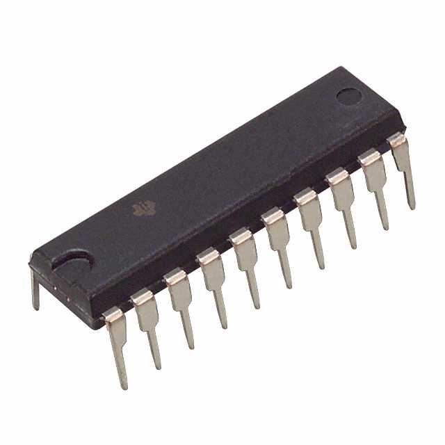
CD74FCT273E
ActiveBICMOS FCT INTERFACE LOGIC OCTAL D-TYPE FLIP-FLOPS WITH RESET
Deep-Dive with AI
Search across all available documentation for this part.

CD74FCT273E
ActiveBICMOS FCT INTERFACE LOGIC OCTAL D-TYPE FLIP-FLOPS WITH RESET
Deep-Dive with AI
Technical Specifications
Parameters and characteristics for this part
| Specification | CD74FCT273E |
|---|---|
| Clock Frequency | 70 MHz |
| Current - Output High, Low [custom] | 15 mA |
| Current - Output High, Low [custom] | 48 mA |
| Current - Quiescent (Iq) | 8 ÁA |
| Max Propagation Delay @ V, Max CL | 7 ns |
| Mounting Type | Through Hole |
| Number of Bits per Element | 8 |
| Number of Elements | 1 |
| Operating Temperature [Max] | 70 °C |
| Operating Temperature [Min] | 0 °C |
| Output Type | Non-Inverted |
| Package / Case | 20-DIP |
| Package / Case | 7.62 mm |
| Package / Case | 0.3 in |
| Supplier Device Package | 20-PDIP |
| Trigger Type | Positive Edge |
| Type | D-Type |
| Voltage - Supply [Max] | 5.25 V |
| Voltage - Supply [Min] | 4.75 V |
Pricing
Prices provided here are for design reference only. For realtime values and availability, please visit the distributors directly
| Distributor | Package | Quantity | $ | |
|---|---|---|---|---|
| Digikey | Tube | 1 | $ 0.72 | |
| 20 | $ 0.65 | |||
| 40 | $ 0.61 | |||
| 100 | $ 0.50 | |||
| 260 | $ 0.47 | |||
| 500 | $ 0.42 | |||
| 1000 | $ 0.39 | |||
| Texas Instruments | TUBE | 1 | $ 0.99 | |
| 100 | $ 0.76 | |||
| 250 | $ 0.56 | |||
| 1000 | $ 0.40 | |||
Description
General part information
CY74FCT273T Series
The CD74FCT273 is a positive-edge-triggered, D-type flip-flop with a direct clear (CLR\) input. This device uses a small-geometry BiCMOS technology. The output stage is a combination of bipolar and CMOS transistors that limits the output high level to two diode drops below VCC. This resultant lowering of output swing (0 V to 3.7 V) reduces power-bus ringing [a source of electromagnetic interference (EMI)] and minimizes VCCbounce and ground bounce and their effects during simultaneous output switching. The output configuration also enhances switching speed and is capable of sinking 48 mA.
Information at the data (D) inputs meeting the setup time requirements is transferred to the Q outputs on the positive-going edge of the clock (CLK) pulse. Clock triggering occurs at a particular voltage level and is not directly related to the transition time of the positive-going pulse. When CLK is at either the high or low level, the D input has no effect at the output. All eight flip-flops are controlled by a common clock (CLK) and a common reset (CLR\). The outputs are placed in a low state when CLR\ is taken low, independent of the CLK.
The CD74FCT273 is characterized for operation from 0°C to 70°C.
Documents
Technical documentation and resources


