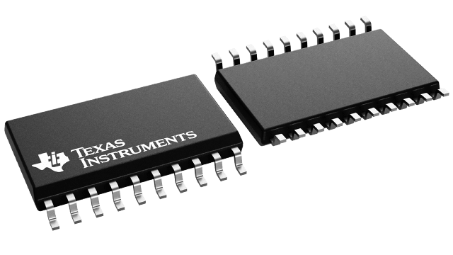
CY74FCT273T Series
BiCMOS FCT Interface Logic Octal D-Type Flip-Flops with Reset
Manufacturer: Texas Instruments
Catalog
BiCMOS FCT Interface Logic Octal D-Type Flip-Flops with Reset
Key Features
• Function, Pinout, and Drive Compatible With FCT and F LogicReduced VOH(Typically = 3.3 V) Versions of Equivalent FCT FunctionsEdge-Rate Control Circuitry for Significantly Improved Noise CharacteristicsIoffSupports Partial-Power-Down Mode OperationMatched Rise and Fall TimesESD Protection Exceeds JESD 222000-V Human-Body Model (A114-A)200-V Machine Model (A115-A)1000-V Charged-Device Model (C101)Fully Compatible With TTL Input and Output Logic LevelsCY54FCT273T32-mA Output Sink Current12-mA Output Source CurrentCY74FCT273T64-mA Output Sink Current32-mA Output Source CurrentFunction, Pinout, and Drive Compatible With FCT and F LogicReduced VOH(Typically = 3.3 V) Versions of Equivalent FCT FunctionsEdge-Rate Control Circuitry for Significantly Improved Noise CharacteristicsIoffSupports Partial-Power-Down Mode OperationMatched Rise and Fall TimesESD Protection Exceeds JESD 222000-V Human-Body Model (A114-A)200-V Machine Model (A115-A)1000-V Charged-Device Model (C101)Fully Compatible With TTL Input and Output Logic LevelsCY54FCT273T32-mA Output Sink Current12-mA Output Source CurrentCY74FCT273T64-mA Output Sink Current32-mA Output Source Current
Description
AI
The CD74FCT273 is a positive-edge-triggered, D-type flip-flop with a direct clear (CLR\) input. This device uses a small-geometry BiCMOS technology. The output stage is a combination of bipolar and CMOS transistors that limits the output high level to two diode drops below VCC. This resultant lowering of output swing (0 V to 3.7 V) reduces power-bus ringing [a source of electromagnetic interference (EMI)] and minimizes VCCbounce and ground bounce and their effects during simultaneous output switching. The output configuration also enhances switching speed and is capable of sinking 48 mA.
Information at the data (D) inputs meeting the setup time requirements is transferred to the Q outputs on the positive-going edge of the clock (CLK) pulse. Clock triggering occurs at a particular voltage level and is not directly related to the transition time of the positive-going pulse. When CLK is at either the high or low level, the D input has no effect at the output. All eight flip-flops are controlled by a common clock (CLK) and a common reset (CLR\). The outputs are placed in a low state when CLR\ is taken low, independent of the CLK.
The CD74FCT273 is characterized for operation from 0°C to 70°C.


