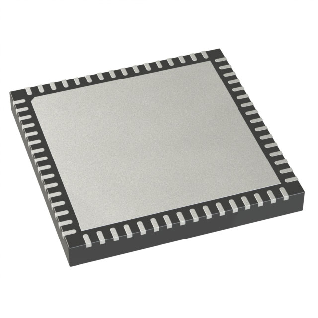
ATMEGA128RFA1-ZUR00
Active2.4GHZ 802.15.4 128K SOC REVF T&R 64 VQFN 9X9X0.9MM T/R ROHS COMPLIANT: YES
Deep-Dive with AI
Search across all available documentation for this part.

ATMEGA128RFA1-ZUR00
Active2.4GHZ 802.15.4 128K SOC REVF T&R 64 VQFN 9X9X0.9MM T/R ROHS COMPLIANT: YES
Deep-Dive with AI
Technical Specifications
Parameters and characteristics for this part
| Specification | ATMEGA128RFA1-ZUR00 |
|---|---|
| Current - Receiving [Max] | 12.5 mA |
| Current - Receiving [Min] | 12 mA |
| Data Rate (Max) | 2 Mbps |
| Frequency | 2.4 GHz |
| GPIO | 38 |
| Memory Size | 16 kB, 4 kB, 128 kB |
| Modulation | O-QPSK |
| Mounting Type | Surface Mount |
| Operating Temperature [Max] | 85 °C |
| Operating Temperature [Min] | -40 °C |
| Package / Case | 64-VFQFN Exposed Pad |
| Power - Output | 3.5 dBm |
| Protocol | Zigbee®, 6LoWPAN |
| RF Family/Standard | 802.15.4 |
| Sensitivity | -100 dBm |
| Serial Interfaces | USART, SPI, JTAG, I2C |
| Supplier Device Package | 64-QFN (9x9) |
| Type | TxRx + MCU |
| Voltage - Supply [Max] | 3.6 V |
| Voltage - Supply [Min] | 1.8 V |
Pricing
Prices provided here are for design reference only. For realtime values and availability, please visit the distributors directly
| Distributor | Package | Quantity | $ | |
|---|---|---|---|---|
| Digikey | Cut Tape (CT) | 1 | $ 8.60 | |
| 25 | $ 7.83 | |||
| 100 | $ 7.83 | |||
| Digi-Reel® | 1 | $ 8.60 | ||
| 25 | $ 7.83 | |||
| 100 | $ 7.83 | |||
| Tape & Reel (TR) | 4000 | $ 7.83 | ||
| Microchip Direct | T/R | 1 | $ 8.60 | |
| 25 | $ 7.83 | |||
| 100 | $ 7.38 | |||
| 1000 | $ 6.59 | |||
| 5000 | $ 6.20 | |||
| Newark | Each (Supplied on Full Reel) | 100 | $ 7.61 | |
Description
General part information
ATmega128RFA1 Series
The high-performance, low-power Microchip 8-bit AVR® RISC-based microcontroller combines 128 KB flash memory with read-while-write capabilities, 4 KB EEPROM, 4 KB SRAM, 53 general purpose I/O lines, 32 general purpose working registers, a real-time counter, four flexible timer/counters with compare modes and PWM, two USARTs, a byte-oriented Two-Wire serial interface, an 8-channel/10-bit A/D converter with optional differential input stage with programmable gain, programmable watchdog timer with internal oscillator, SPI serial port, a JTAG (IEEE® 1149.1 compliant) test interface for accessing the on-chip debugging and programming, and six software selectable power saving modes. The device operates between 2.7-5.5 volts.
By executing powerful instructions in a single clock cycle, the device achieves throughputs approaching one MIPS per MHz, balancing power consumption and processing speed.
Documents
Technical documentation and resources


