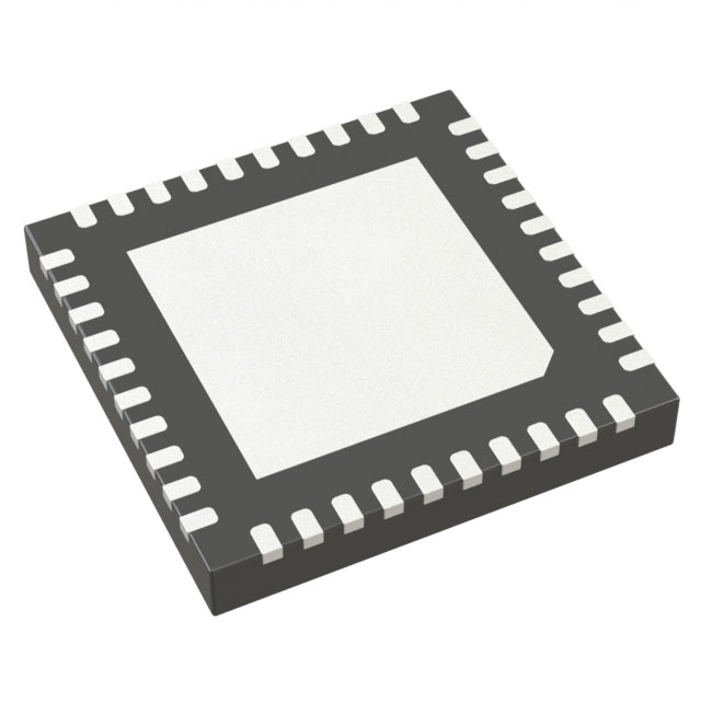
ADRF5515BCPZN
ActiveDUAL-CHANNEL, 3.3 GHZ TO 4.0 GHZ, 20 W RECEIVER FRONT END
Deep-Dive with AI
Search across all available documentation for this part.

ADRF5515BCPZN
ActiveDUAL-CHANNEL, 3.3 GHZ TO 4.0 GHZ, 20 W RECEIVER FRONT END
Deep-Dive with AI
Technical Specifications
Parameters and characteristics for this part
| Specification | ADRF5515BCPZN |
|---|---|
| Frequency [Max] | 4 GHz |
| Frequency [Min] | 3.3 GHz |
| Package / Case | 40-VFQFN Exposed Pad, CSP |
| RF Type | General Purpose |
| Supplier Device Package | 40-LFCSP-VQ (6x6) |
Pricing
Prices provided here are for design reference only. For realtime values and availability, please visit the distributors directly
| Distributor | Package | Quantity | $ | |
|---|---|---|---|---|
| Digikey | Strip | 1 | $ 20.29 | |
| 10 | $ 17.69 | |||
| 25 | $ 16.78 | |||
| 100 | $ 15.54 | |||
| 250 | $ 14.80 | |||
| 500 | $ 14.28 | |||
Description
General part information
ADRF5515 Series
The ADRF5515 is a dual-channel, integrated RF, front-end, multichip module designed for time division duplexing (TDD) applications. The device operates from 3.3 GHz to 4.0 GHz. The ADRF5515 is configured in dual channels with a cascading, two-stage, LNA and a high power silicon SPDT switch.In high gain mode, the cascaded two-stage LNA and switch offer a low noise figure of 1.0 dB and a high gain of 33 dB at 3.6 GHz with an output third-order intercept point (OIP3) of 32 dBm (typical). In low gain mode, one stage of the two-stage LNA is in bypass, providing 16 dB of gain at a lower current of 36 mA. In power-down mode, the LNAs are turned off and the device draws 12 mA.In transmit operation, when RF inputs are connected to a termination pin (TERM-CHA or TERM-CHB), the switch provides low insertion loss of 0.45 dB and handles long-term evolution (LTE) average power (9 dB peak to average ratio (PAR)) of 43 dBm for full lifetime operation.The ADRF5515 is pin-compatible with the ADRF5545A, 10 W version, which operates from 2.4 GHz to 4.2 GHz.The ADRF5515 does not require any matching components at the RF ports that are internally matched to 50 Ω. The ANT and TERM ports are also internally ac-coupled. Therefore, only receiver ports require external dc blocking capacitors.The device comes in an RoHS compliant, compact, 6 mm×6 mm, 40-lead LFCSP package.ApplicationsWireless infrastructureTDD massive multiple input and multiple output and active antenna systemsTDD-based communications systems
Documents
Technical documentation and resources


