ADRF5515 Series
Dual-Channel, 3.3 GHz to 4.0 GHz, 20 W Receiver Front End
Manufacturer: Analog Devices
Catalog
Dual-Channel, 3.3 GHz to 4.0 GHz, 20 W Receiver Front End
Key Features
• Integrated dual-channel RF front end2-stage LNA and high power silicon SPDT switchOn-chip bias and matchingSingle supply operation
• 2-stage LNA and high power silicon SPDT switch
• On-chip bias and matching
• Single supply operation
• GainHigh gain mode: 33 dB typical at 3.6 GHzLow gain mode: 16 dB typical at 3.6 GHz
• High gain mode: 33 dB typical at 3.6 GHz
• Low gain mode: 16 dB typical at 3.6 GHz
• Low noise figureHigh gain mode: 1.0 dB typical at 3.6 GHzLow gain mode: 1.0 dB typical at 3.6 GHz
• High gain mode: 1.0 dB typical at 3.6 GHz
• Low gain mode: 1.0 dB typical at 3.6 GHz
• High isolationRXOUT-CHA and RXOUT-CHB: 45 dB typicalTERM-CHA and TERM-CHB: 60 dB typical
• RXOUT-CHA and RXOUT-CHB: 45 dB typical
• TERM-CHA and TERM-CHB: 60 dB typical
• Low insertion loss: 0.45 dB typical at 3.6 GHz
• High power handling at TCASE= 105°CFull lifetimeLTE average power (9 dB PAR): 43 dBmHigh OIP3 (high gain mode): 32 dBm typicalPower-down mode and low gain mode for LNALow supply currentHigh gain mode: 86 mA typical at 5VLow gain mode: 36 mA typical at 5VPower-down mode: 12 mA typical at 5VPositive logic control6 mm×6 mm, 40-lead LFCSP packagePin compatible with the ADRF5545A, 10 W version
• Full lifetimeLTE average power (9 dB PAR): 43 dBm
• LTE average power (9 dB PAR): 43 dBm
• High OIP3 (high gain mode): 32 dBm typical
• Power-down mode and low gain mode for LNA
• Low supply currentHigh gain mode: 86 mA typical at 5VLow gain mode: 36 mA typical at 5VPower-down mode: 12 mA typical at 5V
• High gain mode: 86 mA typical at 5V
• Low gain mode: 36 mA typical at 5V
• Power-down mode: 12 mA typical at 5V
• Positive logic control
• 6 mm×6 mm, 40-lead LFCSP package
• Pin compatible with the ADRF5545A, 10 W version
Description
AI
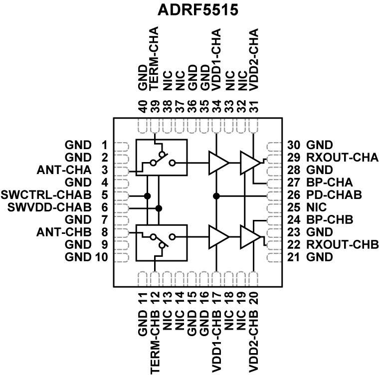
The ADRF5515 is a dual-channel, integrated RF, front-end, multichip module designed for time division duplexing (TDD) applications. The device operates from 3.3 GHz to 4.0 GHz. The ADRF5515 is configured in dual channels with a cascading, two-stage, LNA and a high power silicon SPDT switch.In high gain mode, the cascaded two-stage LNA and switch offer a low noise figure of 1.0 dB and a high gain of 33 dB at 3.6 GHz with an output third-order intercept point (OIP3) of 32 dBm (typical). In low gain mode, one stage of the two-stage LNA is in bypass, providing 16 dB of gain at a lower current of 36 mA. In power-down mode, the LNAs are turned off and the device draws 12 mA.In transmit operation, when RF inputs are connected to a termination pin (TERM-CHA or TERM-CHB), the switch provides low insertion loss of 0.45 dB and handles long-term evolution (LTE) average power (9 dB peak to average ratio (PAR)) of 43 dBm for full lifetime operation.The ADRF5515 is pin-compatible with the ADRF5545A, 10 W version, which operates from 2.4 GHz to 4.2 GHz.The ADRF5515 does not require any matching components at the RF ports that are internally matched to 50 Ω. The ANT and TERM ports are also internally ac-coupled. Therefore, only receiver ports require external dc blocking capacitors.The device comes in an RoHS compliant, compact, 6 mm×6 mm, 40-lead LFCSP package.ApplicationsWireless infrastructureTDD massive multiple input and multiple output and active antenna systemsTDD-based communications systems


