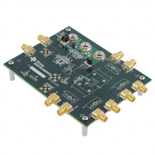
CDCLVD1213EVM
ObsoleteCDCLVD1213 CLOCK BUFFER AND DRIVER EVALUATION BOARD
Deep-Dive with AI
Search across all available documentation for this part.

CDCLVD1213EVM
ObsoleteCDCLVD1213 CLOCK BUFFER AND DRIVER EVALUATION BOARD
Deep-Dive with AI
Technical Specifications
Parameters and characteristics for this part
| Specification | CDCLVD1213EVM |
|---|---|
| Embedded | False |
| Function | Clock Buffer |
| Supplied Contents | Board(s) |
| Type | Timing |
| Utilized IC / Part | CDCLVD1213 |
Pricing
Prices provided here are for design reference only. For realtime values and availability, please visit the distributors directly
| Distributor | Package | Quantity | $ | |
|---|---|---|---|---|
| Digikey | Box | 1 | $ 178.80 | |
Description
General part information
CDCLVD1213 Series
The CDCLVD1213 clock buffer distributes an input clock to 4 pairs of differential LVDS clock outputs with low additive jitter for clock distribution. The input can either be LVDS, LVPECL, or CML.
The CDCLVD1213 contains a high performance divider for one output (QD) which can divide the input clock signal by a factor of 1, 2, or 4.
The CDCLVD1213 is specifically designed for driving 50-Ω transmission lines. The part supports a fail-safe function. The device incorporates an input hysteresis which prevents random oscillation of the outputs in the absence of an input signal.
Documents
Technical documentation and resources


