Deep-Dive with AI
Search across all available documentation for this part.

Deep-Dive with AI
Technical Specifications
Parameters and characteristics for this part
| Specification | CD4043BPWG4 |
|---|---|
| Circuit | 1:1 |
| Current - Output High, Low [custom] | 6.8 mA |
| Current - Output High, Low [custom] | 6.8 mA |
| Delay Time - Propagation | 50 ns |
| Independent Circuits | 4 |
| Logic Type | S-R Latch |
| Mounting Type | Surface Mount |
| Operating Temperature [Max] | 125 °C |
| Operating Temperature [Min] | -55 °C |
| Output Type | Tri-State |
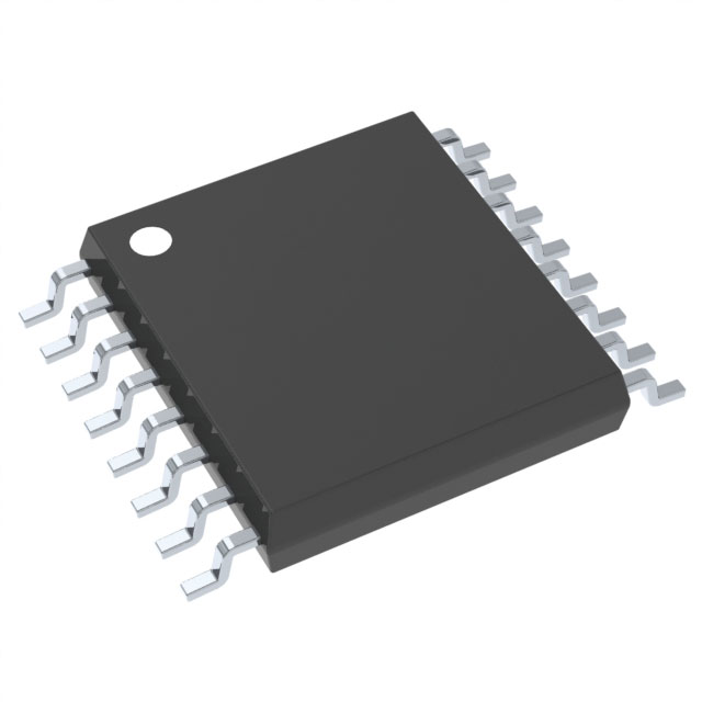
| Package / Case | 16-TSSOP |
| Package / Case [x] | 0.173 in |
| Package / Case [y] | 4.4 mm |
| Supplier Device Package | 16-TSSOP |
| Voltage - Supply [Max] | 18 V |
| Voltage - Supply [Min] | 3 V |
Pricing
Prices provided here are for design reference only. For realtime values and availability, please visit the distributors directly
| Distributor | Package | Quantity | $ | |
|---|---|---|---|---|
Description
General part information
CD4043B Series
CD4043B types are quad cross-coupled 3-state CMOS NOR latches and the CD4044B types are quad cross-coupled 3-state CMOS NAND latches. Each latch has a separate Q output and individual SET and RESET inputs. The Q outputs are controlled by a common ENABLE input. A logic "1" or high on the ENABLE input connects the latch states to the Q outputs. A logic "0" or low on the ENABLE input disconnects the latch states from the Q outputs, resulting in an open circuit condition on the Q outputs. The open circuit feature allows common busing of the outputs.
The CD4043B and CD4044B types are supplied in 16-lead hermetic dual-in-line ceramic packages (F3A suffix), 16-lead dual-in-line plastic packages (E suffix), 16-lead small-outline package (D, DR, DT, DWR, and NSR suffixes), and 16-lead thin shrink small-outline packages (PW and PWR suffixes).
CD4043B types are quad cross-coupled 3-state CMOS NOR latches and the CD4044B types are quad cross-coupled 3-state CMOS NAND latches. Each latch has a separate Q output and individual SET and RESET inputs. The Q outputs are controlled by a common ENABLE input. A logic "1" or high on the ENABLE input connects the latch states to the Q outputs. A logic "0" or low on the ENABLE input disconnects the latch states from the Q outputs, resulting in an open circuit condition on the Q outputs. The open circuit feature allows common busing of the outputs.
Documents
Technical documentation and resources
No documents available


