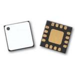
ADCLK914BCPZ-R7
ActiveCLOCK FANOUT BUFFER 1-OUT 1-IN 1:1 16-PIN LFCSP EP T/R
Deep-Dive with AI
Search across all available documentation for this part.

ADCLK914BCPZ-R7
ActiveCLOCK FANOUT BUFFER 1-OUT 1-IN 1:1 16-PIN LFCSP EP T/R
Technical Specifications
Parameters and characteristics for this part
| Specification | ADCLK914BCPZ-R7 |
|---|---|
| Differential - Input:Output [custom] | True |
| Differential - Input:Output [custom] | True |
| Frequency - Max [Max] | 7.5 GHz |
| Input | LVPECL, CMOS, LVDS, CML, LVTTL |
| Mounting Type | Surface Mount |
| Number of Circuits | 1 |
| Operating Temperature [Max] | 125 °C |
| Operating Temperature [Min] | -40 °C |
| Output | HVDS |
| Ratio - Input:Output [custom] | 1:1 |
| Supplier Device Package | 16-LFCSP-VQ (3x3) |
| Type | Buffer/Driver, Data |
| Voltage - Supply [Max] | 3.63 V |
| Voltage - Supply [Min] | 2.97 V |
Pricing
Prices provided here are for design reference only. For realtime values and availability, please visit the distributors directly
| Distributor | Package | Quantity | $ | |
|---|---|---|---|---|
| Digikey | Cut Tape (CT) | 1 | $ 21.18 | |
| 10 | $ 15.45 | |||
| 25 | $ 13.98 | |||
| 100 | $ 12.34 | |||
| 250 | $ 11.55 | |||
| 500 | $ 11.25 | |||
| Digi-Reel® | 1 | $ 21.18 | ||
| 10 | $ 15.45 | |||
| 25 | $ 13.98 | |||
| 100 | $ 12.34 | |||
| 250 | $ 11.55 | |||
| 500 | $ 11.25 | |||
| Tape & Reel (TR) | 1500 | $ 11.25 | ||
Description
General part information
ADCLK914 Series
The ADCLK914 is an ultrafast clock/data buffer fabricated on the Analog Devices, Inc., proprietary, complementary bipolar (XFCB-3) silicon-germanium (SiGe) process. The ADCLK914 features high voltage differential signaling (HVDS) outputs suitable for driving the latest Analog Devices high speed digitalto-analog converters (DACs). The ADCLK914 has a single, differential open-collector output.The ADCLK914 buffer operates up to 7.5 GHz with a 160 ps propagation delay and adds only 110 fs random jitter (RJ). The input has a center tapped, 100 Ω, on-chip termination resistor and accepts LVPECL, CML, CMOS, LVTTL, or LVDS (ac-coupled only). A VREFpin is available for biasing ac-coupled inputs.The HVDS output stage is designed to directly drive 1.9 V each side into 50 Ω terminated to VCCfor a total differential output swing of 3.8 V.The ADCLK914 is available in a 16-lead LFCSP. It is specified for operation over the extended industrial temperature range of −40°C to +125°C.ApplicationsClock and data signal restorationHigh speed converter clockingBroadband communicationsCellular infrastructureHigh speed line receiversATE and high performance instrumentationLevel shiftingThreshold detection
Documents
Technical documentation and resources


