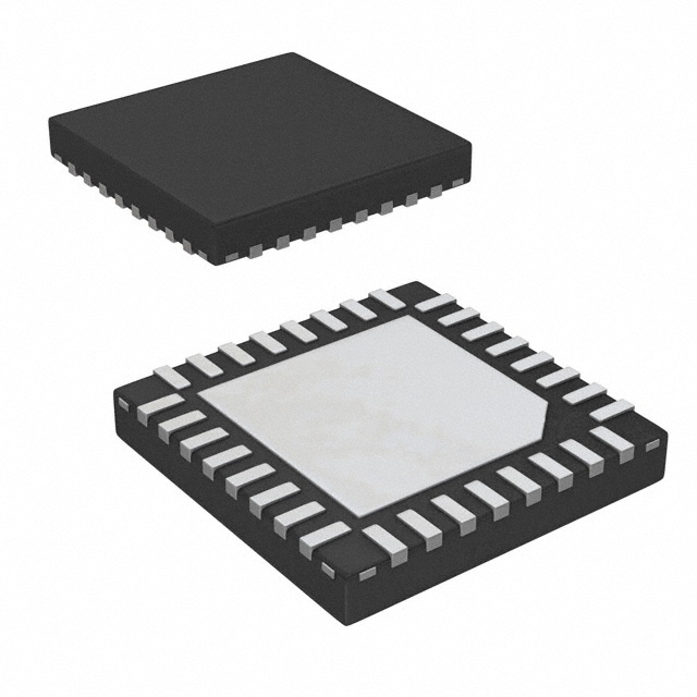
LMK00334RTVR
Active4-OUTPUT PCIE® GEN1/GEN2/GEN3/GEN4/GEN5 CLOCK BUFFER AND LEVEL TRANSLATOR
Deep-Dive with AI
Search across all available documentation for this part.

LMK00334RTVR
Active4-OUTPUT PCIE® GEN1/GEN2/GEN3/GEN4/GEN5 CLOCK BUFFER AND LEVEL TRANSLATOR
Technical Specifications
Parameters and characteristics for this part
| Specification | LMK00334RTVR |
|---|---|
| Differential - Input:Output [custom] | True |
| Differential - Input:Output [custom] | True |
| Frequency - Max [Max] | 400 MHz |
| Input | HSTL, SSTL, LVDS, Crystal, LVPECL, CML, HCSL |
| Main Purpose | PCI Express (PCIe), SATA CPU |
| Mounting Type | Surface Mount |
| Number of Circuits | 1 |
| Operating Temperature [Max] | 85 °C |
| Operating Temperature [Min] | -40 °C |
| Output | HCSL, LVCMOS |
| PLL | False |
| Ratio - Input:Output | 3:5 |
| Supplier Device Package | 32-WQFN (5x5) |
| Voltage - Supply [Max] | 3.45 V |
| Voltage - Supply [Min] | 3.15 V |
Pricing
Prices provided here are for design reference only. For realtime values and availability, please visit the distributors directly
| Distributor | Package | Quantity | $ | |
|---|---|---|---|---|
| Digikey | Cut Tape (CT) | 1 | $ 2.82 | |
| 10 | $ 2.53 | |||
| 25 | $ 2.39 | |||
| 100 | $ 2.03 | |||
| 250 | $ 1.91 | |||
| 500 | $ 1.67 | |||
| Digi-Reel® | 1 | $ 2.82 | ||
| 10 | $ 2.53 | |||
| 25 | $ 2.39 | |||
| 100 | $ 2.03 | |||
| 250 | $ 1.91 | |||
| 500 | $ 1.67 | |||
| Tape & Reel (TR) | 1000 | $ 1.38 | ||
| 2000 | $ 1.29 | |||
| 5000 | $ 1.24 | |||
| Texas Instruments | LARGE T&R | 1 | $ 1.91 | |
| 100 | $ 1.67 | |||
| 250 | $ 1.17 | |||
| 1000 | $ 0.94 | |||
Description
General part information
LMK00334-Q1 Series
The LMK00334 -Q1 device is a 4-output HCSL fanout buffer intended for high-frequency, low-jitter clock, data distribution, and level translation. It is capable of distributing the reference clock for ADCs, DACs, multi-gigabit ethernet, XAUI, fibre channel, SATA/SAS, SONET/SDH, CPRI, and high-frequency backplanes.
The input clock can be selected from two universal inputs or one crystal input. The selected input clock is distributed to two banks of two HCSL outputs and one LVCMOS output. The LVCMOS output has a synchronous enable input for runt-pulse-free operation when enabled or disabled. The LMK00334 -Q1 operates from a 3.3-V core supply and three independent 3.3-V or 2.5-V output supplies.
The LMK00334 -Q1 provides high performance, versatility, and power efficiency, making it ideal for replacing fixed-output buffer devices while increasing timing margin in the system.
Documents
Technical documentation and resources


