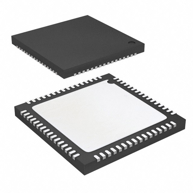
AD7770ACPZ-RL
Active8-CHANNEL, 24-BIT, 32 KSPS SIMULTANEOUS SAMPLING ADC
Deep-Dive with AI
Search across all available documentation for this part.

AD7770ACPZ-RL
Active8-CHANNEL, 24-BIT, 32 KSPS SIMULTANEOUS SAMPLING ADC
Deep-Dive with AI
Technical Specifications
Parameters and characteristics for this part
| Specification | AD7770ACPZ-RL |
|---|---|
| Architecture | Sigma-Delta |
| Configuration | MUX-PGA-ADC |
| Data Interface | SPI |
| Features | Simultaneous Sampling, PGA |
| Input Type | Single Ended, Differential |
| Mounting Type | Surface Mount |
| Number of A/D Converters | 8 |
| Number of Bits | 24 |
| Number of Inputs | 8 |
| Operating Temperature [Max] | 125 °C |
| Operating Temperature [Min] | -40 °C |
| Package / Case | 64-WFQFN Exposed Pad, CSP |
| Ratio - S/H:ADC | 1:1 |
| Reference Type | External, Internal |
| Sampling Rate (Per Second) | 32 k per second |
| Supplier Device Package | 64-LFCSP (9x9) |
| Voltage - Supply, Analog [Max] | 3.6 V |
| Voltage - Supply, Analog [Min] | 2.2 V |
Pricing
Prices provided here are for design reference only. For realtime values and availability, please visit the distributors directly
| Distributor | Package | Quantity | $ | |
|---|---|---|---|---|
| Digikey | Cut Tape (CT) | 1 | $ 21.32 | |
| 10 | $ 15.20 | |||
| 25 | $ 13.60 | |||
| 100 | $ 12.45 | |||
| Digi-Reel® | 1 | $ 21.32 | ||
| 10 | $ 15.20 | |||
| 25 | $ 13.60 | |||
| 100 | $ 12.45 | |||
| Tape & Reel (TR) | 2500 | $ 12.45 | ||
Description
General part information
AD7770 Series
The AD7770 is an 8-channel, simultaneous sampling ADC. Eight full sigma-delta (Σ-Δ) ADCs are on chip. The AD7770 provides a low input current to allow direct sensor connection. Each input channel has a programmable gain stage allowing gains of 1, 2, 4, and 8 to map lower amplitude sensor outputs into the full-scale ADC input range, maximizing the dynamic range of the signal chain. The AD7770 accepts a VREF voltage from 1 V up to 3.6 V.The analog inputs accept unipolar (0 V to VREF) or true bipolar (±VREF/2) analog input signals with 3.3 V or ±1.65 V analog supply voltages, respectively for PGAGAIN= 1. The analog inputs can be configured to accept true differential, pseudo differential, or single-ended signals to match different sensor output configurations.Each channel contains a PGA, an ADC modulator and a sinc3, low latency digital filter. An SRC is provided to allow fine resolution control over the AD7770 ODR. This control can be used in applications where the ODR resolution is required to maintain coherency with 0.01 Hz changes in the line frequency. The SRC is programmable through the serial port interface (SPI). The AD7770 implements two different interfaces: a data output interface and SPI control interface. The ADC data output interface is dedicated to transmitting the ADC conversion results from the AD7770 to the processor. The SPI writes to and reads from the AD7770 configuration registers and for the control and reading of data from the SAR ADC. The SPI can also be configured to output the Σ-Δ conversion data.The AD7770 includes a 12-bit SAR ADC. This ADC can be used for AD7770 diagnostics without having to decommission one of the Σ-Δ ADC channels dedicated to system measurement functions. With the use of an external multiplexer, which can be controlled through the three general-purpose input/output pins (GPIOs), and signal conditioning, the SAR ADC can validate the Σ-Δ ADC measurements in applications where functional safety is required. In addition, the AD7770 SAR ADC includes an internal multiplexer to sense internal nodes.The AD7770 contains a 2.5 V reference and reference buffer. The reference has a typical temperature coefficient of 10 ppm/°C.The AD7770 offers two modes of operation: high resolution mode and low power mode. High resolution mode provides a higher dynamic range while consuming 10.75 mW per channel; low power mode consumes just 3.37 mW per channel at a reduced dynamic range specification.The specified operating temperature range is −40°C to +105°C, although the device is operational up to +125°C.ApplicationsProtection relaysGeneral-purpose data acquisitionIndustrial process control
Documents
Technical documentation and resources


