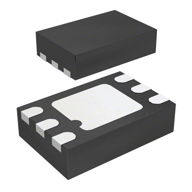
AD5611ACPZ-RL7
Active2.7 V TO 5.5 V, <100 ΜA, 10-BITNANODAC, SPI INTERFACE IN LFCSP AND SC70
Deep-Dive with AI
Search across all available documentation for this part.

AD5611ACPZ-RL7
Active2.7 V TO 5.5 V, <100 ΜA, 10-BITNANODAC, SPI INTERFACE IN LFCSP AND SC70
Deep-Dive with AI
Technical Specifications
Parameters and characteristics for this part
| Specification | AD5611ACPZ-RL7 |
|---|---|
| Architecture | String DAC |
| Data Interface | DSP, SPI |
| Differential Output | False |
| INL/DNL (LSB) | ±0.5, ±4 |
| Mounting Type | Surface Mount |
| Number of Bits [custom] | 10 |
| Operating Temperature [Max] | 125 °C |
| Operating Temperature [Min] | -40 °C |
| Output Type | Voltage - Buffered |
| Package / Case | 6-VDFN Exposed Pad, CSP |
| Reference Type | Supply |
| Settling Time | 10 µs |
| Supplier Device Package | 6-LFCSP-WD (2x3) |
| Voltage - Supply, Analog [Max] | 5.5 V |
| Voltage - Supply, Analog [Min] | 2.7 V |
| Voltage - Supply, Digital [Max] | 5.5 V |
| Voltage - Supply, Digital [Min] | 2.7 V |
Pricing
Prices provided here are for design reference only. For realtime values and availability, please visit the distributors directly
| Distributor | Package | Quantity | $ | |
|---|---|---|---|---|
| Digikey | Cut Tape (CT) | 1 | $ 3.15 | |
| Digi-Reel® | 1 | $ 3.15 | ||
| Tape & Reel (TR) | 3000 | $ 0.93 | ||
Description
General part information
AD5611 Series
TheAD5601/AD5611/AD5621, members of thenanoDAC®family, are single, 8-/10-/12-bit, buffered voltage output DACs that operate from a single 2.7 V to 5.5 V supply, consuming typically 75 μA at 5 V. The parts come in tiny LFCSP and SC70 packages. Their on-chip precision output amplifier allows rail-to-rail output swing to be achieved. The AD5601/AD5611/AD5621 utilize a versatile 3-wire serial interface that operates at clock rates up to 30 MHz and is compatible with SPI, QSPI™, MICROWIRE™, and DSP interface standards.The reference for the AD5601/AD5611/AD5621 is derived from the power supply inputs and, therefore, gives the widest dynamic output range. The parts incorporate a power-on reset circuit, which ensures that the DAC output powers up to 0 V and remains there until a valid write to the device takes place.The AD5601/AD5611/AD5621 contain a power-down feature that reduces current consumption to typically 0.2 μA at 3 V.They also provide software-selectable output loads while in power-down mode. The parts are put into power-down mode over the serial interface.The low power consumption of these parts in normal operation makes them ideally suited to portable battery-operated equip-ment. The combination of small package and low power makes thesenanoDAC devices ideal for level-setting requirements, such as generating bias or control voltages in space-constrained and power-sensitive applications.Product HighlightsAvailable in 6-lead LFCSP and SC70 packages.Low power, single-supply operation. The AD5601/ AD5611/AD5621 operate from a single 2.7 V to 5.5 V supply with a maximum current consumption of 100 μA, making them ideal for battery-powered applications.The on-chip output buffer amplifier allows the output of the DAC to swing rail-to-rail with a typical slew rate of 0.5 V/μs.Reference is derived from the power supply.High speed serial interface with clock speeds up to 30 MHz. Designed for very low power consumption. The interface powers up only during a write cycle.Power-down capability. When powered down, the DAC typically consumes 0.2 μA at 3 V. Power-on reset with brownout detection.ApplicationsVoltage level settingPortable battery-powered instrumentsDigital gain and offset adjustmentProgrammable voltage and current sourcesProgrammable attenuators
Documents
Technical documentation and resources


