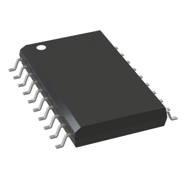
SY100EL29VZG
ActiveFLIP FLOP, D, 700 PS, 1.1 GHZ, 50 MA, 20 PINS, WSOIC
Deep-Dive with AI
Search across all available documentation for this part.

SY100EL29VZG
ActiveFLIP FLOP, D, 700 PS, 1.1 GHZ, 50 MA, 20 PINS, WSOIC
Deep-Dive with AI
Technical Specifications
Parameters and characteristics for this part
| Specification | SY100EL29VZG |
|---|---|
| Clock Frequency | 1.1 GHz |
| Current - Quiescent (Iq) | 50 mA |
| Function | Set(Preset) and Reset |
| Mounting Type | Surface Mount |
| Number of Bits per Element | 1 bits |
| Number of Elements | 2 |
| Operating Temperature (Max) | 85 °C |
| Operating Temperature (Min) | -40 °C |
| Output Type | Differential |
| Package Length | 0.295 in |
| Package Name | 20-SOIC |
| Package Width | 7.5 mm |
| Trigger Type | Positive Edge |
| Type | D-Type |
| Voltage - Supply (Maximum) | -3 V |
| Voltage - Supply (Minimum) | -5.5 V |
Pricing
Prices provided here are for design reference only. For realtime values and availability, please visit the distributors directly
| Distributor | Package | Quantity | $ | Updated |
|---|---|---|---|---|
| Digikey | Tube | 1 | $ 4.91 | <2d |
| 25 | $ 4.09 | |||
| 100 | $ 3.95 | |||
| Microchip Direct | TUBE | 1 | $ 4.91 | 1m+ |
| 25 | $ 4.09 | |||
| 100 | $ 3.72 | |||
| 1000 | $ 3.59 | |||
| 5000 | $ 3.55 | |||
| 10000 | $ 3.51 | |||
CAD
3D models and CAD resources for this part
Description
General part information
100EL29 Series
The SY100EL29V is a dual differential register with differential data (inputs and outputs) and clock. The registers are triggered by a positive transition of the positive clock (CLK) input. A HIGH on the Reset (Rx) asynchronously resets the appropriate register so that the Q outputs go LOW. A HIGH on the Set (Sx) asynchronously resets the appropriate register so that the Q outputs go HIGH. The Set and Reset inputs cannot both be HIGH simultaneously. The differential input structures are clamped so that the inputs of unused registers can be left open without upsetting the bias network of the devices. The clamping action will assert the /D and the /CLK sides of the inputs. The noninverting input will pull down to VEE and the inverting input will be biased around VCC/2. Because of the edge-triggered flip-flop nature of the devices, simultaneously opening both the clock and data inputs will result in an output which reaches an unidentified but valid state. The fully differential design of the devices makes them ideal for very high frequency applications where a registered data path is necessary.3.3V and 5V power supply option Differential D, CLK and Q Extended VEE range of –3.0V to –5.5V VBB output for single-ended use 1100MHz min. toggle frequency Asynchronous Reset and Set Available in 20-pin SOIC package
Documents
Technical documentation and resources

