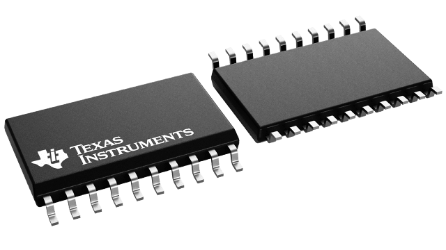
TLV5632IDW
Active8-BIT 8-CH. 1/3 US DAC, SER. INPUT, PGRMABLE SETTLING TIME/POWER CONSUMP, LOW POWER, PWRDN, INT REF
Deep-Dive with AI
Search across all available documentation for this part.

TLV5632IDW
Active8-BIT 8-CH. 1/3 US DAC, SER. INPUT, PGRMABLE SETTLING TIME/POWER CONSUMP, LOW POWER, PWRDN, INT REF
Deep-Dive with AI
Technical Specifications
Parameters and characteristics for this part
| Specification | TLV5632IDW |
|---|---|
| Architecture | String DAC |
| Data Interface | SPI |
| Differential Output | False |
| INL/DNL (LSB) | 0.1 LSB, 0.3 LSB |
| Mounting Type | Surface Mount |
| Number of Bits | 8 |
| Number of D/A Converters | 8 |
| Operating Temperature [Max] | 85 °C |
| Operating Temperature [Min] | -40 °C |
| Output Type | Voltage - Buffered |
| Package / Case | 20-SOIC |
| Package / Case [y] | 0.295 in |
| Package / Case [y] | 7.5 mm |
| Reference Type | External, Internal |
| Settling Time | 7 µs |
| Supplier Device Package | 20-SOIC |
| Voltage - Supply, Analog | 5 V |
| Voltage - Supply, Analog [Max] | 3.3 V |
| Voltage - Supply, Analog [Min] | 2.7 V |
| Voltage - Supply, Digital | 5 V |
| Voltage - Supply, Digital [Max] | 3.3 V |
| Voltage - Supply, Digital [Min] | 2.7 V |
Pricing
Prices provided here are for design reference only. For realtime values and availability, please visit the distributors directly
| Distributor | Package | Quantity | $ | |
|---|---|---|---|---|
| Digikey | Tube | 100 | $ 8.37 | |
| Texas Instruments | TUBE | 1 | $ 9.36 | |
| 100 | $ 7.63 | |||
| 250 | $ 6.00 | |||
| 1000 | $ 5.09 | |||
Description
General part information
TLV5632 Series
The TLV5630, TLV5631, and TLV5632 are pin-compatible, eight-channel, 12-/10-/8-bit voltage output DACs each with a flexible serial interface. The serial interface allows glueless interface to TMS320 and SPI, QSPI, and Microwire serial ports. It is programmed with a 16-bit serial string containing 4 control and 12 data bits.
Additional features are a power-down mode, anLDACinput for simultaneous update of all eight DAC outputs, and a data output which can be used to cascade multiple devices, and an internal programmable band-gap reference.
The resistor string output voltage is buffered by a rail-to-rail output amplifier with a programmable settling time to allow the designer to optimize speed vs power dissipation. The buffered, high-impedance reference input can be connected to the supply voltage.
Documents
Technical documentation and resources


