Deep-Dive with AI
Search across all available documentation for this part.

Technical Specifications
Parameters and characteristics for this part
| Specification | AD9852ASTZ |
|---|---|
| Master fclk | 200 MHz |
| Mounting Type | Surface Mount |
| Operating Temperature [Max] | 85 °C |
| Operating Temperature [Min] | -40 °C |
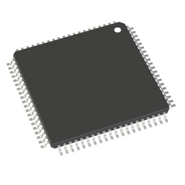
| Package / Case | 80-LQFP |
| Resolution (Bits) | 12 b |
| Supplier Device Package | 80-LQFP |
| Supplier Device Package [x] | 14 |
| Supplier Device Package [y] | 14 |
| Tuning Word Width (Bits) | 48 b |
| Voltage - Supply [Max] | 3.47 V |
| Voltage - Supply [Min] | 3.14 V |
Pricing
Prices provided here are for design reference only. For realtime values and availability, please visit the distributors directly
| Distributor | Package | Quantity | $ | |
|---|---|---|---|---|
| Digikey | Tray | 1 | $ 66.87 | |
| 10 | $ 52.52 | |||
| 25 | $ 48.86 | |||
| 80 | $ 46.17 | |||
Description
General part information
AD9852 Series
The AD9852 digital synthesizer is a highly integrated device that uses advanced DDS technology, coupled with an internal high speed, high performance D/A converter to form a digitally programmable, agile synthesizer function. When referenced to an accurate clock source, the AD9852 generates a highly stable frequency-, phase-, and amplitude-programmable cosine output that can be used as an agile LO in communications, radar, and many other applications. The innovative high speed DDS core of the AD9852 provides 48-bit frequency resolution (1 μHz tuning resolution with 300 MHz SYSCLK). Retaining 16 bits for phase-to-amplitude conversion ensures excellent spurious-free dynamic range (SFDR).The circuit architecture of the AD9852 allows the generation of output signals at frequencies up to 150 MHz, which can be digitally tuned at a rate of up to 100 million new frequencies per second. The (externally filtered) cosine wave output can be converted to a square wave by the internal comparator for agile clock generator applications. The device provides two 14-bit phase registers and a single pin for BPSK operation.For higher-order PSK operation, the I/O interface can be used for phase changes. The 12-bit cosine DAC, coupled with the innovative DDS architecture, provides excellent wideband and narrow-band output SFDR. When configured with the comparator, the 12-bit control DAC facilitates static duty cycle control in the high speed clock generator applications.The 12-bit digital multiplier permits programmable amplitude modulation, on/off output shaped keying, and precise amplitude control of the cosine DAC output. Chirp functionality is also included for wide bandwidth frequency sweeping applications. The AD9852 programmable 4× to 20× REFCLK multiplier circuit internally generates the 300 MHz system clock from a lower frequency external reference clock. This saves the user the expense and difficulty of implementing a 300 MHz system clock source.Direct 300 MHz clocking is also accommodated with either single-ended or differential inputs. Single-pin, conventional FSK and the enhanced spectral qualities of ramped FSK are supported. The AD9852 uses advanced 0.35 μ CMOS technology to provide this high level of functionality on a single 3.3 V supply.The AD9852 is pin-for-pin compatible with the AD9854 single-tone synthesizer. The AD9852 is specified to operate over the extended industrial temperature range of −40°C to +85°C.ApplicationsAgile LO frequency synthesisProgrammable clock generatorFM chirp source for radar and scanning systemsTest and measurement equipmentCommercial and amateur RF exciter
Documents
Technical documentation and resources


