Catalog
CMOS 300 MSPS Complete DDS
Key Features
• 300 MHz internal clock rate
• FSK, BPSK, PSK, chirp, AM operation
• Dual integrated 12-bit D/A converters
• Ultrahigh speed comparator, 3 ps rms jitter
• Excellent dynamic performance80 dB SFDR at 100 MHz (±1 MHz) AOUT
• 80 dB SFDR at 100 MHz (±1 MHz) AOUT
• 4× to 20× programmable reference clock multiplier
• Dual 48-bit programmable frequency registers
• Dual 14-bit programmable phase offset registers
• 12-bit programmable amplitude modulation and on/off output shaped keying function
• Single-pin FSK and BPSK data interfaces
• PSK capability via I/O interface
• Linear or nonlinear FM chirp functions with single pin frequency hold function
• Frequency ramped FSK
• <25 ps rms total jitter in clock generator mode
• Automatic bidirectional frequency sweeping
• Sin(x)/x correction
• Simplified control interface10 MHz serial 2-wire or 3-wire SPI-compatible100 MHz parallel 8-bit programming
• 10 MHz serial 2-wire or 3-wire SPI-compatible
• 100 MHz parallel 8-bit programming
• 3.3 V single supply
• Multiple power-down functions
• Single-ended or differential input reference clock
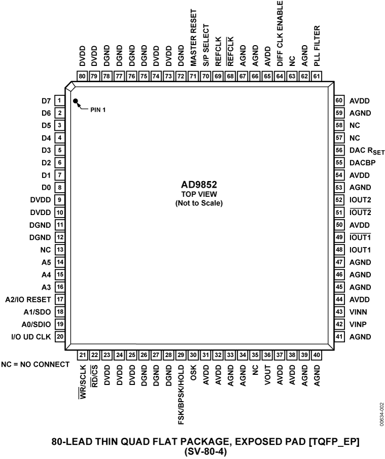
• Small, 80-lead LQFP or TQFP with exposed pad
Description
AI
The AD9852 digital synthesizer is a highly integrated device that uses advanced DDS technology, coupled with an internal high speed, high performance D/A converter to form a digitally programmable, agile synthesizer function. When referenced to an accurate clock source, the AD9852 generates a highly stable frequency-, phase-, and amplitude-programmable cosine output that can be used as an agile LO in communications, radar, and many other applications. The innovative high speed DDS core of the AD9852 provides 48-bit frequency resolution (1 μHz tuning resolution with 300 MHz SYSCLK). Retaining 16 bits for phase-to-amplitude conversion ensures excellent spurious-free dynamic range (SFDR).The circuit architecture of the AD9852 allows the generation of output signals at frequencies up to 150 MHz, which can be digitally tuned at a rate of up to 100 million new frequencies per second. The (externally filtered) cosine wave output can be converted to a square wave by the internal comparator for agile clock generator applications. The device provides two 14-bit phase registers and a single pin for BPSK operation.For higher-order PSK operation, the I/O interface can be used for phase changes. The 12-bit cosine DAC, coupled with the innovative DDS architecture, provides excellent wideband and narrow-band output SFDR. When configured with the comparator, the 12-bit control DAC facilitates static duty cycle control in the high speed clock generator applications.The 12-bit digital multiplier permits programmable amplitude modulation, on/off output shaped keying, and precise amplitude control of the cosine DAC output. Chirp functionality is also included for wide bandwidth frequency sweeping applications. The AD9852 programmable 4× to 20× REFCLK multiplier circuit internally generates the 300 MHz system clock from a lower frequency external reference clock. This saves the user the expense and difficulty of implementing a 300 MHz system clock source.Direct 300 MHz clocking is also accommodated with either single-ended or differential inputs. Single-pin, conventional FSK and the enhanced spectral qualities of ramped FSK are supported. The AD9852 uses advanced 0.35 μ CMOS technology to provide this high level of functionality on a single 3.3 V supply.The AD9852 is pin-for-pin compatible with the AD9854 single-tone synthesizer. The AD9852 is specified to operate over the extended industrial temperature range of −40°C to +85°C.ApplicationsAgile LO frequency synthesisProgrammable clock generatorFM chirp source for radar and scanning systemsTest and measurement equipmentCommercial and amateur RF exciter


