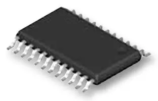
AD5340BRUZ
ActiveDIGITAL TO ANALOG CONVERTER, 12 BIT, PARALLEL, 2.5V TO 5.5V, TSSOP, 24 PINS
Deep-Dive with AI
Search across all available documentation for this part.

AD5340BRUZ
ActiveDIGITAL TO ANALOG CONVERTER, 12 BIT, PARALLEL, 2.5V TO 5.5V, TSSOP, 24 PINS
Deep-Dive with AI
Technical Specifications
Parameters and characteristics for this part
| Specification | AD5340BRUZ |
|---|---|
| Architecture | String DAC |
| Data Interface | Parallel |
| Differential Output | False |
| INL/DNL (LSB) | 0.2 LSB, 2 LSB |
| Mounting Type | Surface Mount |
| Number of Bits | 12 bits |
| Operating Temperature [Max] | 105 ░C |
| Operating Temperature [Min] | -40 °C |
| Output Type | Voltage - Buffered |
| Package / Case | 24-TSSOP |
| Package / Case | 0.173 in, 4.4 mm |
| Reference Type | External |
| Settling Time | 10 µs |
| Supplier Device Package | 24-TSSOP |
| Voltage - Supply, Analog [Max] | 5.5 V |
| Voltage - Supply, Analog [Min] | 2.5 V |
| Voltage - Supply, Digital [Max] | 5.5 V |
| Voltage - Supply, Digital [Min] | 2.5 V |
Pricing
Prices provided here are for design reference only. For realtime values and availability, please visit the distributors directly
Description
General part information
AD5340 Series
TheAD5330/AD5331/ AD5340 /AD5341are single 8-/10-/12-bit DACs. They operate from a 2.5 V to 5.5 V supply consuming just 115 μA at 3 V and feature a power-down mode that further reduces the current to 80 nA. The devices incorporate an on-chip output buffer that can drive the output to both supply rails, but the AD5330, AD5340, and AD5341 allow a choice of buffered or unbuffered reference input.The AD5330 / AD5331 / AD5340 / AD5341 have a parallel interface.CSselects the device and data is loaded into the input registers on the rising edge ofWR.The GAIN pin allows the output range to be set at 0 V to VREFor 0 V to 2 × VREF.Input data to the DACs is double-buffered, allowing simultaneous update of multiple DACs in a system using theLDACpin.An asynchronousCLRinput is also provided, which resets the contents of the input register and the DAC register to all zeros. These devices also incorporate a power-on reset circuit that ensures that the DAC output powers on to 0 V and remains there until valid data is written to the device.The AD5330 / AD5331 / AD5340 / AD5341 are available in thin shrink small outline packages (TSSOP).APPLICATIONSPortable battery-powered instrumentsDigital gain and offset adjustmentProgrammable voltage and current sourcesProgrammable attenuatorsIndustrial process control


