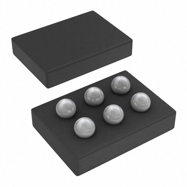
CSD75208W1015
Active-20-V, P CHANNEL NEXFET™ POWER MOSFET, DUAL COMMON SOURCE WLP 1 MM X 1.5 MM, 108 MOHM, GATE ESD PROT
Deep-Dive with AI
Search across all available documentation for this part.

CSD75208W1015
Active-20-V, P CHANNEL NEXFET™ POWER MOSFET, DUAL COMMON SOURCE WLP 1 MM X 1.5 MM, 108 MOHM, GATE ESD PROT
Deep-Dive with AI
Technical Specifications
Parameters and characteristics for this part
| Specification | CSD75208W1015 |
|---|---|
| Configuration | 2 P-Channel (Dual) Common Source |
| Current - Continuous Drain (Id) @ 25°C | 1.6 A |
| Drain to Source Voltage (Vdss) | 20 V |
| FET Feature | Logic Level Gate |
| Input Capacitance (Ciss) (Max) @ Vds [Max] | 410 pF |
| Mounting Type | Surface Mount |
| Operating Temperature [Max] | 150 °C |
| Operating Temperature [Min] | -55 °C |
| Package / Case | DSBGA, 6-UFBGA |
| Power - Max [Max] | 750 mW |
| Rds On (Max) @ Id, Vgs | 68 mOhm |
| Supplier Device Package | 6-DSBGA (1x1.5) |
| Technology | MOSFET (Metal Oxide) |
| Vgs(th) (Max) @ Id | 1.1 V |
Pricing
Prices provided here are for design reference only. For realtime values and availability, please visit the distributors directly
| Distributor | Package | Quantity | $ | |
|---|---|---|---|---|
| Digikey | Cut Tape (CT) | 1 | $ 0.54 | |
| 10 | $ 0.46 | |||
| 100 | $ 0.32 | |||
| 500 | $ 0.25 | |||
| 1000 | $ 0.20 | |||
| Digi-Reel® | 1 | $ 0.54 | ||
| 10 | $ 0.46 | |||
| 100 | $ 0.32 | |||
| 500 | $ 0.25 | |||
| 1000 | $ 0.20 | |||
| Tape & Reel (TR) | 3000 | $ 0.18 | ||
| 6000 | $ 0.17 | |||
| 9000 | $ 0.16 | |||
| 30000 | $ 0.16 | |||
| Texas Instruments | LARGE T&R | 1 | $ 0.32 | |
| 100 | $ 0.21 | |||
| 250 | $ 0.17 | |||
| 1000 | $ 0.11 | |||
Description
General part information
CSD75208W1015 Series
This device is designed to deliver the lowest on-resistance and gate charge in the smallest outline possible with excellent thermal characteristics in an ultra-low profile. Low on-resistance coupled with the small footprint and low profile make the device ideal for battery operated space constrained applications.
This device is designed to deliver the lowest on-resistance and gate charge in the smallest outline possible with excellent thermal characteristics in an ultra-low profile. Low on-resistance coupled with the small footprint and low profile make the device ideal for battery operated space constrained applications.
Documents
Technical documentation and resources


