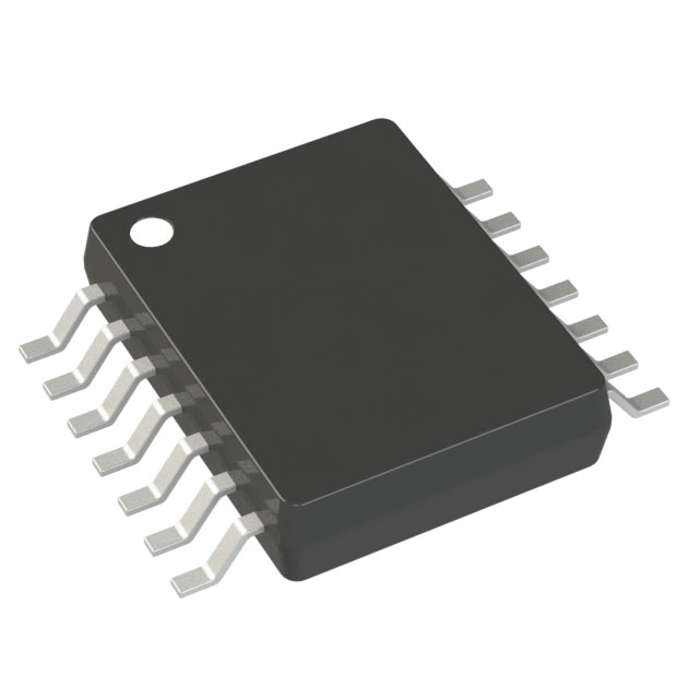
AD5025BRUZ
ActiveFULLY ACCURATE 12-BIT VOUTNANODAC®SPI INTERFACE 4.5 V TO 5.5 V IN A TSSOP
Deep-Dive with AI
Search across all available documentation for this part.

AD5025BRUZ
ActiveFULLY ACCURATE 12-BIT VOUTNANODAC®SPI INTERFACE 4.5 V TO 5.5 V IN A TSSOP
Deep-Dive with AI
Technical Specifications
Parameters and characteristics for this part
| Specification | AD5025BRUZ |
|---|---|
| Architecture | R-2R |
| Data Interface | DSP, SPI |
| Differential Output | False |
| INL/DNL (LSB) | 0.2 LSB, 0.05 LSB |
| Mounting Type | Surface Mount |
| Number of Bits | 12 bits |
| Operating Temperature [Max] | 125 °C |
| Operating Temperature [Min] | -40 °C |
| Output Type | Voltage - Buffered |
| Package / Case | 14-TSSOP |
| Package / Case [custom] | 0.173 " |
| Package / Case [custom] | 4.4 mm |
| Reference Type | External |
| Settling Time | 13 µs |
| Supplier Device Package | 14-TSSOP |
| Voltage - Supply, Analog | 5 V |
| Voltage - Supply, Digital | 5 V |
Pricing
Prices provided here are for design reference only. For realtime values and availability, please visit the distributors directly
| Distributor | Package | Quantity | $ | |
|---|---|---|---|---|
| Digikey | Tube | 1 | $ 16.60 | |
| 10 | $ 11.92 | |||
| 25 | $ 10.72 | |||
| 100 | $ 9.37 | |||
| 250 | $ 8.72 | |||
| 500 | $ 8.33 | |||
| 1000 | $ 8.26 | |||
Description
General part information
AD5025 Series
The AD5025 /AD5045/AD5065are low power, dual 12-/14-/16-bit buffered voltage output nanoDAC®DACs offering relative accuracy specifications of ±1 LSB INL with individual reference pins, and can operate from a single 4.5 V to 5.5 V supply. The AD5025 / AD5045 / AD5065 also offer a differential accuracy specification of ±1 LSB. The parts use a versatile 3-wire, low power Schmitt trigger serial interface that operates at clock rates up to 50 MHz and is compatible with standard SPI®, QSPI™, MICROWIRE™, and DSP interface standards. The reference for the AD5025 / AD5045 / AD5065 are supplied from an external pin and a reference buffer is provided on chip. The AD5025 / AD5045 / AD5065 incorporate a power-on reset circuit that ensures the DAC output powers up zero scale or midscale and remains there until a valid write takes place to the device. The AD5025 / AD5045 / AD5065 contain a power-down feature that reduces the current consumption of the device to typically 400 nA at 5 V and provides software selectable output loads while in power-down mode. The parts are put into power-down mode over the serial interface. Total unadjusted error for the parts is <2.5 mV. The parts exhibit very low glitch on power-up. The outputs of all DACs can be updated simultaneously using theLDACfunction, with the added functionality of user-selectable DAC channels to simultaneously update. There is also an asynchronousCLRthat clears all DACs to a software-selectable code—0 V, midscale, or full scale. The parts also feature a power-down lockout pin,PDL, which can be used to prevent the DAC from entering power-down under any circumstances over the serial interface.Product HighlightsDual channel available in a 14-lead TSSOP package with individual voltage reference pins.12-/14-/16-bit accurate, ±1 LSB INL.Low glitch on power-up.High speed serial interface with clock speeds up to 50 MHz.Three power-down modes available to the user.Reset to known output voltage (zero scale or midscale).Power-down lockout capability.ApplicationsProcess controlsData acquisition systemsPortable battery-powered instrumentsDigital gain and offset adjustmentProgrammable voltage and current sourcesProgrammable attenuators
Documents
Technical documentation and resources


