AD5025 Series
Fully Accurate 12-Bit VOUTnanoDAC®SPI Interface 4.5 V to 5.5 V in a TSSOP
Manufacturer: Analog Devices
Catalog
Fully Accurate 12-Bit VOUTnanoDAC®SPI Interface 4.5 V to 5.5 V in a TSSOP
Key Features
• Low power dual 12-/14-/16-bit DAC, ±1 LSB INL
• Individual voltage reference pins
• Rail-to-rail operation
• 4.5 V to 5.5 V power supply
• Power-on reset to zero scale or midscale
• Power down to 400 nA at 5 V
• 3 power-down functions
• Per channel power-down
• Low glitch upon power-up
• Hardware power-down lockout capability
• HardwareLDACwith softwareLDACoverride function
• CLRfunction to programmable code
• SDO daisy-chaining option
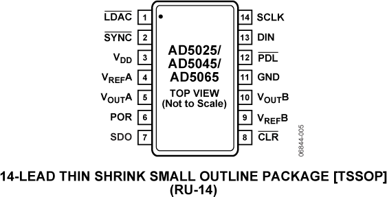
• 14-lead TSSOP
Description
AI
The AD5025 /AD5045/AD5065are low power, dual 12-/14-/16-bit buffered voltage output nanoDAC®DACs offering relative accuracy specifications of ±1 LSB INL with individual reference pins, and can operate from a single 4.5 V to 5.5 V supply. The AD5025 / AD5045 / AD5065 also offer a differential accuracy specification of ±1 LSB. The parts use a versatile 3-wire, low power Schmitt trigger serial interface that operates at clock rates up to 50 MHz and is compatible with standard SPI®, QSPI™, MICROWIRE™, and DSP interface standards. The reference for the AD5025 / AD5045 / AD5065 are supplied from an external pin and a reference buffer is provided on chip. The AD5025 / AD5045 / AD5065 incorporate a power-on reset circuit that ensures the DAC output powers up zero scale or midscale and remains there until a valid write takes place to the device. The AD5025 / AD5045 / AD5065 contain a power-down feature that reduces the current consumption of the device to typically 400 nA at 5 V and provides software selectable output loads while in power-down mode. The parts are put into power-down mode over the serial interface. Total unadjusted error for the parts is <2.5 mV. The parts exhibit very low glitch on power-up. The outputs of all DACs can be updated simultaneously using theLDACfunction, with the added functionality of user-selectable DAC channels to simultaneously update. There is also an asynchronousCLRthat clears all DACs to a software-selectable code—0 V, midscale, or full scale. The parts also feature a power-down lockout pin,PDL, which can be used to prevent the DAC from entering power-down under any circumstances over the serial interface.Product HighlightsDual channel available in a 14-lead TSSOP package with individual voltage reference pins.12-/14-/16-bit accurate, ±1 LSB INL.Low glitch on power-up.High speed serial interface with clock speeds up to 50 MHz.Three power-down modes available to the user.Reset to known output voltage (zero scale or midscale).Power-down lockout capability.ApplicationsProcess controlsData acquisition systemsPortable battery-powered instrumentsDigital gain and offset adjustmentProgrammable voltage and current sourcesProgrammable attenuators


