ADG1634LYCPZ-REEL7
Active4.7 Ω RON, QUAD SPDT SWITCH WITH 1.2 V AND 1.8 V JEDEC LOGIC COMPLIANCE
Deep-Dive with AI
Search across all available documentation for this part.

ADG1634LYCPZ-REEL7
Active4.7 Ω RON, QUAD SPDT SWITCH WITH 1.2 V AND 1.8 V JEDEC LOGIC COMPLIANCE
Technical Specifications
Parameters and characteristics for this part
| Specification | ADG1634LYCPZ-REEL7 |
|---|---|
| -3db Bandwidth | 77 MHz |
| Channel Capacitance (CS(off), CD(off)) [custom] | 32 pF |
| Channel Capacitance (CS(off), CD(off)) [custom] | 19 pF |
| Channel-to-Channel Matching (ΔRon) | 120 mOhm |
| Charge Injection | -12.4 pC |
| Crosstalk | -64 dB |
| Current - Leakage (IS(off)) (Max) [Max] | 150 pA |
| Mounting Type | Surface Mount |
| Multiplexer/Demultiplexer Circuit | 2:1 |
| Number of Circuits | 4 |
| On-State Resistance (Max) [Max] | 4.6 Ohm |
| Operating Temperature [Max] | 125 °C |
| Operating Temperature [Min] | -40 °C |
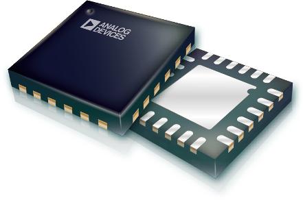
| Package / Case | 24-VFQFN Exposed Pad, CSP |
| Supplier Device Package | 24-LFCSP (4x4) |
| Switch Circuit | SPDT |
| Switch Time (Ton, Toff) (Max) [custom] | 154 ns |
| Switch Time (Ton, Toff) (Max) [custom] | 195 ns |
| Voltage - Supply, Dual (V±) | 8 V, 3.3 V |
| Voltage - Supply, Single (V+) [Max] | 16 V |
| Voltage - Supply, Single (V+) [Min] | 3.3 V |
Pricing
Prices provided here are for design reference only. For realtime values and availability, please visit the distributors directly
Description
General part information
ADG1634L Series
The ADG1634L is a monolithic industrial CMOS (iCMOS®) analog switch comprising four independently selectable single-pole, double-throw (SPDT) switches, respectively.All channels exhibit break-before-make switching action that prevents momentary shorting when switching channels. An EN input on the ADG1634L is used to enable or disable the device. When disabled, all channels are switched off. The switch is enabled with a Logic 1 EN input, while the INx input defines the state of the SPDT switch (see Table 12 in the data sheet).The ultralow on resistance and on-resistance flatness of the switch makes it an ideal solution for data acquisition and gain switching applications, where low distortion is critical.iCMOS construction ensures ultra low power dissipation, making the device ideally suited for portable and battery-powered instruments.An external VLsupply provides flexibility for lower logic control. The ADG1634L is both 1.2 V and 1.8 V JEDEC standard compliant.APPLICATIONSCommunication systemsMedical systemsAudio signal routingVideo signal routingAutomatic test equipmentData acquisition systemsBattery-powered systemsFPGA and microcontroller systemsSample-and-hold systemsRelay replacementsPRODUCT HIGHLIGHTS8.2 Ω maximum on resistance over temperature.Minimum distortion.VLsupply for low logic level compatibility.JEDEC standard compliant for both 1.2 V and 1.8 V logic levels.Guaranteed switch off when digital inputs are floating.24-lead, 4 mm × 4 mm LFCSP.
Documents
Technical documentation and resources


