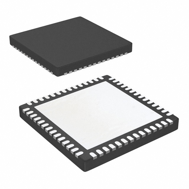
AD9230BCPZ11-200
Active11-BIT, 200 MSPS, 1.8 V ANALOG-TO-DIGITAL CONVERTER
Deep-Dive with AI
Search across all available documentation for this part.

AD9230BCPZ11-200
Active11-BIT, 200 MSPS, 1.8 V ANALOG-TO-DIGITAL CONVERTER
Deep-Dive with AI
Technical Specifications
Parameters and characteristics for this part
| Specification | AD9230BCPZ11-200 |
|---|---|
| Architecture | Pipelined |
| Configuration | S/H-ADC |
| Data Interface | LVDS - Parallel |
| Input Type | Single Ended, Differential |
| Mounting Type | Surface Mount |
| Number of A/D Converters | 1 |
| Number of Bits | 11 |
| Number of Inputs | 1 |
| Operating Temperature [Max] | 85 °C |
| Operating Temperature [Min] | -40 °C |
| Package / Case | 56-VFQFN Exposed Pad, CSP |
| Ratio - S/H:ADC | 1:1 |
| Reference Type | Internal |
| Sampling Rate (Per Second) | 200 M |
| Supplier Device Package | 56-LFCSP-VQ (8x8) |
| Voltage - Supply, Analog [Max] | 1.9 V |
| Voltage - Supply, Analog [Min] | 1.7 V |
| Voltage - Supply, Digital [Max] | 1.9 V |
| Voltage - Supply, Digital [Min] | 1.7 V |
Pricing
Prices provided here are for design reference only. For realtime values and availability, please visit the distributors directly
| Distributor | Package | Quantity | $ | |
|---|---|---|---|---|
| Digikey | Tray | 9 | $ 71.74 | |
| 18 | $ 68.08 | |||
| 27 | $ 66.24 | |||
| 81 | $ 64.90 | |||
Description
General part information
AD9230-11 Series
The AD9230-11 is an 11-bit monolithic sampling analog-to-digital converter (ADC) optimized for high performance, low power, and ease of use. The product operates at up to a 200 MSPS conversion rate and is optimized for outstanding dynamic performance in wideband carrier and broadband systems. All necessary functions, including a track-and-hold (T/H) amplifier and voltage reference, are included on the chip to provide a complete signal conversion solution.The ADC requires a 1.8 V analog voltage supply and a differential clock for full performance operation. The digital outputs are LVDS (ANSI-644) compatible and support twos complement, offset binary format, or Gray code. A data clock output is available for proper output data timing.Fabricated on an advanced CMOS process, the AD9230-11 is available in a 56-lead lead frame chip scale package, specified over the industrial temperature range (−40°C to +85°C).Product HighlightsHigh Performance. Maintains 62.5 dBFS SNR @ 200 MSPS with a 70 MHz input.Low Power. Consumes only 373 mW @ 200 MSPS.Ease of Use. LVDS output data and output clock signal allow interface to current FPGA technology. The on-chip reference and sample-and-hold provide flexibility in system design. Use of a single 1.8 V supply simplifies system power supply design.Serial Port Control. Standard serial port interface (SPI) supports various product functions, such as data formatting, disabling the clock duty cycle stabilizer, power-down, gain adjust, and output test pattern generation.Pin-Compatible Family. 10-bit and 12-bit pin-compatible family offered asAD9211andAD9230.ApplicationsWireless and wired broadband communicationsCable reverse pathCommunications test equipmentRadar and satellite subsystemsPower amplifier linearization
Documents
Technical documentation and resources


