AD9230-11 Series
12-Bit, 170 MSPS/210 MSPS/250 MSPS, 1.8 V Analog-to-Digital Converter
Manufacturer: Analog Devices
Catalog
12-Bit, 170 MSPS/210 MSPS/250 MSPS, 1.8 V Analog-to-Digital Converter
Key Features
• SNR = 64.9 dBFS @ fINup to 70 MHz @ 250 MSPS
• ENOB of 10.4 @ fINup to 70 MHz @ 250 MSPS (−1.0 dBFS)
• SFDR = −79 dBc @ fINup to 70 MHz @ 250 MSPS (−1.0 dBFS)
• Excellent linearityDNL = ±0.3 LSB typicalINL = ±0.5 LSB typical
• 700 MHz full power analog bandwidth
• On-chip reference, no external decoupling required
• Integrated input buffer and track-and-hold
• Low power dissipation434 mW @ 250 MSPS—LVDS SDR mode400 mW @ 250 MSPS—LVDS DDR mode
• Programmable input voltage range 1.0 V to 1.5 V, 1.25 V nominal
• 1.8 V analog and digital supply operation
• LVDS output with selectable data format(offset binary, twos complement, Gray code)
• 11-bit version available: AD923011BCPZ-200
• High Performance—Maintains 64.9 dBFS SNR @ 250 MSPS with a 70 MHz input.
• Low Power—Consumes only 434 mW @ 250 MSPS.
• Ease of Use—LVDS output data and output clock signal allow interface to current FPGA technology. The on-chip reference and sample and hold provide flexibility in system design. Use of a single 1.8 V supply simplifies system power supply design.
• Serial Port Control—Standard serial port interface supports various product functions, such as data formatting, disabling the clock duty cycle stabilizer, power-down, gain adjust, and output test pattern generation.
• Pin-Compatible Family—10-bit pin-compatible family offered as AD9211.
• Wireless and wired broadband communications
• Cable reverse path
• Communications test equipment
• Radar and satellite subsystems
• Power amplifier linearization
Description
AI
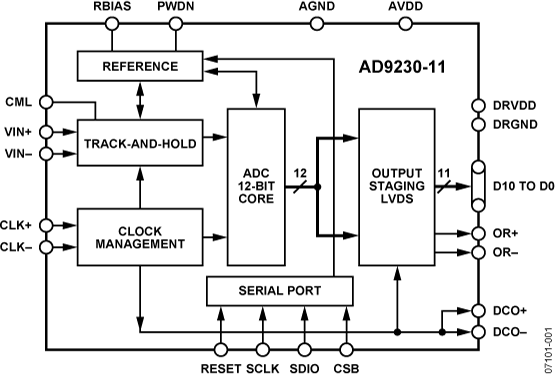
The AD9230-11 is an 11-bit monolithic sampling analog-to-digital converter (ADC) optimized for high performance, low power, and ease of use. The product operates at up to a 200 MSPS conversion rate and is optimized for outstanding dynamic performance in wideband carrier and broadband systems. All necessary functions, including a track-and-hold (T/H) amplifier and voltage reference, are included on the chip to provide a complete signal conversion solution.The ADC requires a 1.8 V analog voltage supply and a differential clock for full performance operation. The digital outputs are LVDS (ANSI-644) compatible and support twos complement, offset binary format, or Gray code. A data clock output is available for proper output data timing.Fabricated on an advanced CMOS process, the AD9230-11 is available in a 56-lead lead frame chip scale package, specified over the industrial temperature range (−40°C to +85°C).Product HighlightsHigh Performance. Maintains 62.5 dBFS SNR @ 200 MSPS with a 70 MHz input.Low Power. Consumes only 373 mW @ 200 MSPS.Ease of Use. LVDS output data and output clock signal allow interface to current FPGA technology. The on-chip reference and sample-and-hold provide flexibility in system design. Use of a single 1.8 V supply simplifies system power supply design.Serial Port Control. Standard serial port interface (SPI) supports various product functions, such as data formatting, disabling the clock duty cycle stabilizer, power-down, gain adjust, and output test pattern generation.Pin-Compatible Family. 10-bit and 12-bit pin-compatible family offered asAD9211andAD9230.ApplicationsWireless and wired broadband communicationsCable reverse pathCommunications test equipmentRadar and satellite subsystemsPower amplifier linearization


