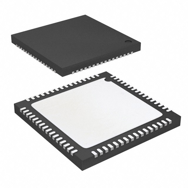
AD9650BCPZRL7-25
Active16-BIT, 25 MSPS/65 MSPS/80 MSPS/105 MSPS, 1.8 V DUAL ANALOG-TO-DIGITAL CONVERTER (ADC)
Deep-Dive with AI
Search across all available documentation for this part.

AD9650BCPZRL7-25
Active16-BIT, 25 MSPS/65 MSPS/80 MSPS/105 MSPS, 1.8 V DUAL ANALOG-TO-DIGITAL CONVERTER (ADC)
Deep-Dive with AI
Technical Specifications
Parameters and characteristics for this part
| Specification | AD9650BCPZRL7-25 |
|---|---|
| Architecture | Pipelined |
| Configuration | S/H-ADC |
| Data Interface | LVDS - Parallel, Parallel |
| Features | Simultaneous Sampling |
| Input Type | Differential |
| Mounting Type | Surface Mount |
| Number of A/D Converters | 2 |
| Number of Bits | 16 |
| Number of Inputs | 2 |
| Operating Temperature [Max] | 85 °C |
| Operating Temperature [Min] | -40 °C |
| Package / Case | 64-VFQFN Exposed Pad, CSP |
| Ratio - S/H:ADC | 1:1 |
| Reference Type | External, Internal |
| Sampling Rate (Per Second) | 25 M |
| Supplier Device Package | 64-LFCSP-VQ (9x9) |
| Voltage - Supply, Analog [Max] | 1.9 V |
| Voltage - Supply, Analog [Min] | 1.7 V |
| Voltage - Supply, Digital [Max] | 1.9 V |
| Voltage - Supply, Digital [Min] | 1.7 V |
Pricing
Prices provided here are for design reference only. For realtime values and availability, please visit the distributors directly
| Distributor | Package | Quantity | $ | |
|---|---|---|---|---|
| Digikey | Tape & Reel (TR) | 750 | $ 91.65 | |
Description
General part information
AD9650 Series
The AD9650 is a dual, 16-bit, 25 MSPS/65 MSPS/80 MSPS/ 105 MSPS analog-to-digital converter (ADC) designed for digitizing high frequency, wide dynamic range signals with input frequencies of up to 300 MHz.The dual ADC core features a multistage, differential pipelined architecture with integrated output error correction logic. Each ADC features wide bandwidth, differential sample-and-hold analog input amplifiers, and shared integrated voltage reference, which eases design considerations. A duty cycle stabilizer is provided to compensate for variations in the ADC clock duty cycle, allowing the converters to maintain excellent performance.The ADC output data can be routed directly to the two external 16-bit output ports or multiplexed on a single 16-bit bus. These outputs can be set to either 1.8 V CMOS or LVDS.Flexible power-down options allow significant power savings, when desired.Programming for setup and control is accomplished using a 3-wire SPI-compatible serial interface.The AD9650 is available in a 64-lead LFCSP and is specified over the industrial temperature range of −40°C to +85°C.PRODUCT HIGHLIGHTSOn-chip dither option for improved SFDR performance with low power analog input.Proprietary differential input that maintains excellent SNR performance for input frequencies up to 300 MHz.Operation from a single 1.8 V supply and a separate digital output driver supply accommodating 1.8 V CMOS or LVDS outputs.Standard serial port interface (SPI) that supports various product features and functions, such as data formatting (offset binary, twos complement, or gray coding), enabling the clock DCS, power-down, and test modes.Pin compatible with the AD9268 and other dual families, AD9269, AD9251, AD9231, and AD9204. This allows a simple migration across resolutions and bandwidth.APPLICATIONSIndustrial instrumentationX-Ray, MRI, and ultrasound equipmentHigh speed pulse acquisitionChemical and spectrum analysisDirect conversion receiversMultimode digital receiversSmart antenna systemsGeneral-purpose software radios
Documents
Technical documentation and resources


