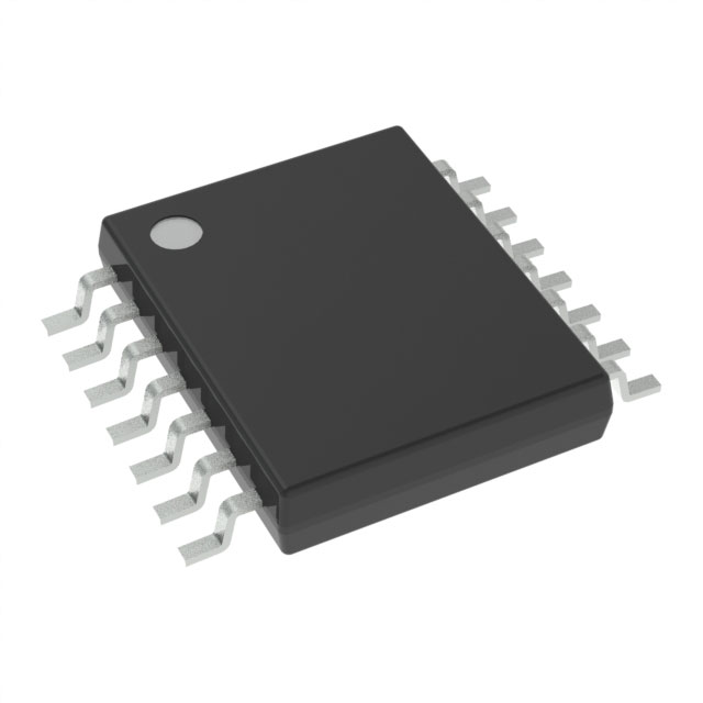
CD4093BPW
Obsolete4-CH, 2-INPUT, 3-V TO 18-V NAND GATES WITH SCHMITT-TRIGGER INPUTS
Deep-Dive with AI
Search across all available documentation for this part.

CD4093BPW
Obsolete4-CH, 2-INPUT, 3-V TO 18-V NAND GATES WITH SCHMITT-TRIGGER INPUTS
Technical Specifications
Parameters and characteristics for this part
| Specification | CD4093BPW |
|---|---|
| Current - Output High, Low [custom] | 3.4 mA |
| Current - Output High, Low [custom] | 3.4 mA |
| Current - Quiescent (Max) [Max] | 4 µA |
| Features | Schmitt Trigger |
| Input Logic Level - High [Max] | 10.8 V |
| Input Logic Level - High [Min] | 3.6 V |
| Input Logic Level - Low [Max] | 4 V |
| Input Logic Level - Low [Min] | 0.9 V |
| Logic Type | NAND Gate |
| Max Propagation Delay @ V, Max CL | 130 ns |
| Mounting Type | Surface Mount |
| Number of Circuits | 4 |
| Number of Inputs | 2 |
| Operating Temperature [Max] | 125 °C |
| Operating Temperature [Min] | -55 °C |
| Package / Case | 14-TSSOP |
| Package / Case [custom] | 0.173 " |
| Package / Case [custom] | 4.4 mm |
| Supplier Device Package | 14-TSSOP |
| Voltage - Supply [Max] | 18 V |
| Voltage - Supply [Min] | 3 V |
Pricing
Prices provided here are for design reference only. For realtime values and availability, please visit the distributors directly
| Distributor | Package | Quantity | $ | |
|---|---|---|---|---|
| Digikey | Tube | 1 | $ 1.13 | |
| 10 | $ 1.01 | |||
| 90 | $ 0.79 | |||
| 270 | $ 0.74 | |||
| 540 | $ 0.65 | |||
| 1080 | $ 0.51 | |||
| 2520 | $ 0.48 | |||
| 5040 | $ 0.46 | |||
| Texas Instruments | TUBE | 1 | $ 0.81 | |
| 100 | $ 0.63 | |||
| 250 | $ 0.46 | |||
| 1000 | $ 0.33 | |||
Description
General part information
CD4093B-Q1 Series
CD4093B consists of four Schmitt-trigger circuits. Each circuit functions as a two-input NAND gate with Schmitt-trigger action on both inputs. The gate switches at different points for positive- and negative-going signals. The difference between the positive voltage (VP) and the negative voltage (VN) is defined as hysteresis voltage (VH) (see Fig. 2).
The CD4093B types are supplied in 14-lead hermetic dual-in-line ceramic packages (F3A suffix), 14-lead dual-in-line plastic packages (E suffix), 14-lead small-outline packages (M, MT, M96, and NSR suffixes), and 14-lead thin shrink small-outline packages (PW and PWR suffixes).
CD4093B consists of four Schmitt-trigger circuits. Each circuit functions as a two-input NAND gate with Schmitt-trigger action on both inputs. The gate switches at different points for positive- and negative-going signals. The difference between the positive voltage (VP) and the negative voltage (VN) is defined as hysteresis voltage (VH) (see Fig. 2).
Documents
Technical documentation and resources


