CD4093B-Q1 Series
Automotive 4-ch, 2-input, 3-V to 18-V NAND gates with Schmitt-Trigger inputs
Manufacturer: Texas Instruments
Catalog
Automotive 4-ch, 2-input, 3-V to 18-V NAND gates with Schmitt-Trigger inputs
Key Features
• Qualified for Automotive ApplicationsSchmitt-Trigger Action on Each Input With No External ComponentsHysteresis Voltage Typically 0.9 V at VDD= 5 V and 2.3 V at VDD= 10 VNoise Immunity Greater Than 50%No Limit on Input Rise and Fall TimesStandardized, Symmetrical Output Characteristics100% Tested for Quiescent Current at 20 VMaximum Input Current of 1µA at 18 V Over Full Package Temperature Range, 100 nA at 18 V and 25°C5-V, 10-V, and 15-V Parametric RatingsESD Protection Level Per AEC-Q100 Classification2000-V (H2) Human-Body Model200-V (M3) Machine-Model1000-V (C5) Charge-Device ModelApplicationsWave and Pulse ShapersHigh-Noise-Environment SystemsMonostable MultivibratorsAstable MultivibratorsNAND LogicQualified for Automotive ApplicationsSchmitt-Trigger Action on Each Input With No External ComponentsHysteresis Voltage Typically 0.9 V at VDD= 5 V and 2.3 V at VDD= 10 VNoise Immunity Greater Than 50%No Limit on Input Rise and Fall TimesStandardized, Symmetrical Output Characteristics100% Tested for Quiescent Current at 20 VMaximum Input Current of 1µA at 18 V Over Full Package Temperature Range, 100 nA at 18 V and 25°C5-V, 10-V, and 15-V Parametric RatingsESD Protection Level Per AEC-Q100 Classification2000-V (H2) Human-Body Model200-V (M3) Machine-Model1000-V (C5) Charge-Device ModelApplicationsWave and Pulse ShapersHigh-Noise-Environment SystemsMonostable MultivibratorsAstable MultivibratorsNAND Logic
Description
AI
CD4093B consists of four Schmitt-trigger circuits. Each circuit functions as a two-input NAND gate with Schmitt-trigger action on both inputs. The gate switches at different points for positive- and negative-going signals. The difference between the positive voltage (VP) and the negative voltage (VN) is defined as hysteresis voltage (VH) (see Fig. 2).
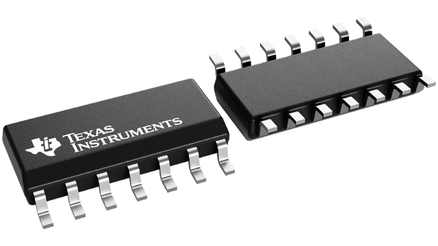
The CD4093B types are supplied in 14-lead hermetic dual-in-line ceramic packages (F3A suffix), 14-lead dual-in-line plastic packages (E suffix), 14-lead small-outline packages (M, MT, M96, and NSR suffixes), and 14-lead thin shrink small-outline packages (PW and PWR suffixes).


