SN74AVC16827 Series
20-ch, 1.2-V to 3.6-V buffers with 3-state outputs
Manufacturer: Texas Instruments
Catalog
20-ch, 1.2-V to 3.6-V buffers with 3-state outputs
Key Features
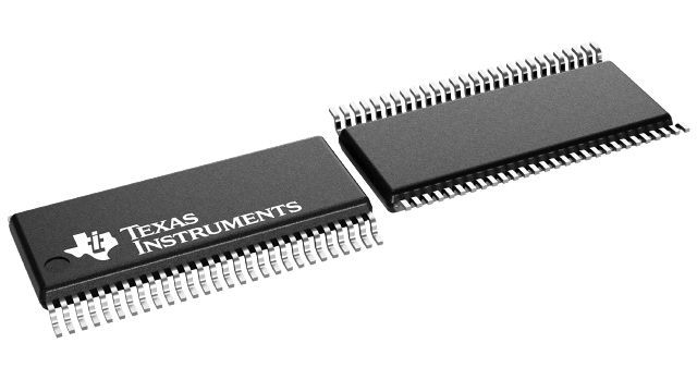
• Member of the Texas InstrumentsWidebusTMFamilyEPICTM(Enhanced-Performance Implanted CMOS) Submicron ProcessDOCTM(Dynamic Output Control) Circuit Dynamically Changes Output Impedance, Resulting in Noise Reduction Without Speed DegradationLess Than 2-ns Maximum Propagation Delay at 2.5-V and 3.3-V VCCDynamic Drive Capability Is Equivalent to Standard Outputs With IOHand IOLof ±24 mA at 2.5-V VCCOvervoltage-Tolerant Inputs/Outputs Allow Mixed-Voltage-Mode Data CommunicationsIoffSupports Partial-Power-Down Mode OperationLatch-Up Performance Exceeds 100 mA Per JESD 78, Class IIPackage Options Include Plastic Thin Shrink Small-Outline (DGG) and Thin Very Small-Outline (DGV) PackagesDOC, EPIC, and Widebus are trademarks of Texas Instruments.Member of the Texas InstrumentsWidebusTMFamilyEPICTM(Enhanced-Performance Implanted CMOS) Submicron ProcessDOCTM(Dynamic Output Control) Circuit Dynamically Changes Output Impedance, Resulting in Noise Reduction Without Speed DegradationLess Than 2-ns Maximum Propagation Delay at 2.5-V and 3.3-V VCCDynamic Drive Capability Is Equivalent to Standard Outputs With IOHand IOLof ±24 mA at 2.5-V VCCOvervoltage-Tolerant Inputs/Outputs Allow Mixed-Voltage-Mode Data CommunicationsIoffSupports Partial-Power-Down Mode OperationLatch-Up Performance Exceeds 100 mA Per JESD 78, Class IIPackage Options Include Plastic Thin Shrink Small-Outline (DGG) and Thin Very Small-Outline (DGV) PackagesDOC, EPIC, and Widebus are trademarks of Texas Instruments.
Description
AI
A Dynamic Output Control (DOC) circuit is implemented, which, during the transition, initially lowers the output impedance to effectively drive the load and, subsequently, raises the impedance to reduce noise. Figure 1 shows typical VOLvs IOLand VOHvs IOHcurves to illustrate the output impedance and drive capability of the circuit. At the beginning of the signal transition, the DOC circuit provides a maximum dynamic drive that is equivalent to a high-drive standard-output device. For more information, refer to the TI application reports,AVC Logic Family Technology and Applications, literature number SCEA006, andDynamic Output Control (DOCTM) Circuitry Technology and Applications, literature number SCEA009.
This 20-bit noninverting buffer/driver is operational at 1.2-V to 3.6-V VCC, but is designed specifically for 1.65-V to 3.6-V VCCoperation.
The SN74AVC16827 is composed of two 10-bit sections with separate output-enable signals. For either 10-bit buffer section, the two output-enable (1OE1\ and 1OE2\ or 2OE1\ and 2OE2\) inputs must both be low for the corresponding Y outputs to be active. If either output-enable input is high, the outputs of that 10-bit buffer section are in the high-impedance state.
To ensure the high-impedance state during power up or power down, OE\ should be tied to VCCthrough a pullup resistor; the minimum value of the resistor is determined by the current-sinking capability of the driver.
This device is fully specified for partial-power-down applications using Ioff. The Ioffcircuitry disables the outputs, preventing damaging current backflow through the device when it is powered down.
The SN74AVC16827 is characterized for operation from -40°C to 85°C.


