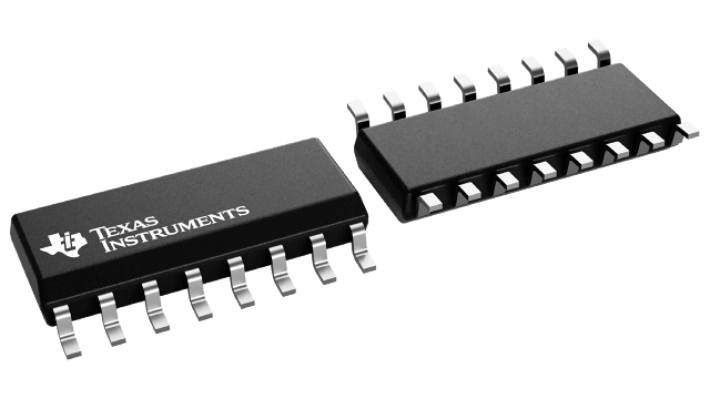
CD74HC112 Series
High Speed CMOS Logic Dual Negative-Edge-Triggered J-K Flip-Flops with Set and Reset
Manufacturer: Texas Instruments
Catalog
High Speed CMOS Logic Dual Negative-Edge-Triggered J-K Flip-Flops with Set and Reset
Key Features
• Wide operating voltage range of 2V to 6VOutputs can drive up to 10 LSTTL loadsLow power consumption, 40µA max ICCTypical tpd = 13ns±4mA output drive at 5VLow input current of 1µA maxWide operating voltage range of 2V to 6VOutputs can drive up to 10 LSTTL loadsLow power consumption, 40µA max ICCTypical tpd = 13ns±4mA output drive at 5VLow input current of 1µA max
Description
AI
The SNx4HC112 devices contain two independent J-K negative-edge-triggered flip-flops. A low level at the preset (PRE) or clear (CLR) inputs sets or resets the outputs, regardless of the levels of the other inputs. When PRE and CLR are inactive (high), data at the J and K inputs meeting the setup time requirements are transferred to the outputs on the negative-going edge of the clock (CLK) pulse. Clock triggering occurs at a voltage level and is not directly related to the fall time of the CLK pulse. Following the hold-time interval, data at the J and K inputs may be changed without affecting the levels at the outputs. These versatile flip-flops perform as toggle flip-flops by tying J and K high.
The SNx4HC112 devices contain two independent J-K negative-edge-triggered flip-flops. A low level at the preset (PRE) or clear (CLR) inputs sets or resets the outputs, regardless of the levels of the other inputs. When PRE and CLR are inactive (high), data at the J and K inputs meeting the setup time requirements are transferred to the outputs on the negative-going edge of the clock (CLK) pulse. Clock triggering occurs at a voltage level and is not directly related to the fall time of the CLK pulse. Following the hold-time interval, data at the J and K inputs may be changed without affecting the levels at the outputs. These versatile flip-flops perform as toggle flip-flops by tying J and K high.


