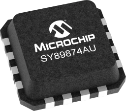
SY89874AU Series
Manufacturer: Microchip Technology
Catalog
Key Features
• * Integrated programmable clock divider and 1:2 fanout buffer
• * >2.5GHz fMAX
• * <250ps tr/tf
• * <15ps within device skew
• * 81fs additive jitter (typical)
• * <10psPP total jitter
• * <1psRMS cycle-to-cycle jitter
• * Unique input termination and VTpin for DC-coupled and AC-coupled Inputs; CML, PECL, LVDS and HSTL
• * TTL/CMOS inputs for select and reset
• * 100k EP compatible LVPECL outputs
• * Parallel programming capability
• * Programmable divider ratios of 1, 2, 4, 8 and 16
• * Low voltage operation 2.5V or 3.3V
• * Output disable function
• * -40°C to 85°C temperature range
• * Available in 16-pin (3mm x 3mm) MLF® package
Description
AI
This low-skew, low-jitter device can accept a high-speed (622MHz or higher) LVTTL, LVCMOS, CML, LVPECL, LVDS or HSTL clock input signal and divide down the frequency using a programmable divider ratio to create a frequency-locked, lower speed version of the input clock. Available divider ratios are 2, 4, 8, and 16, or straight pass-through. In a typical 622MHz clock system this would provide availability of 311MHz, 155MHz, 77MHz, or 38MHz auxiliary clock components.
The differential input buffer has a unique internal termination design that allows access to the termination network through a VT pin. This feature allows the device to easily interface to different logic standards. A VREF-AC reference is included for AC-coupled applications.The /RESET input asynchronously resets the divider. In the pass-through function (divide by 1) the /RESET synchronously enables or disables the outputs on the next falling edge of IN (rising edge of /N).Use the SY89874U version, which has a wider input range, to DC-couple low offset differential signals.


