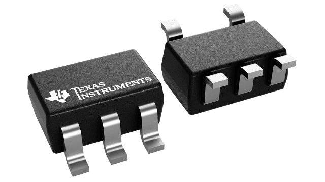
SN74LVC1G79-Q1 Series
Automotive Single Positive-Edge-Triggered D-Type Flip-Flop
Manufacturer: Texas Instruments
Catalog
Automotive Single Positive-Edge-Triggered D-Type Flip-Flop
Key Features
• Available in the Texas InstrumentsNanoFree™ PackageLatch-Up Performance Exceeds 100 mA Per JESD 78, Class IIESD Protection Exceeds JESD 222000-V Human-Body Model (A114-A)200-V Machine Model (A115-A)1000-V Charged-Device Model (C101)Supports 5-V VCCOperationInputs Accept Voltages to 5.5 VSupports Down Translation to VCCMax tpdof 6 ns at 3.3 V and 50 pF loadLow Power Consumption, 10-µA Max ICC±24-mA Output Drive at 3.3 VIoffsupports Partial-Power-Down Mode and Back-Drive ProtectionAvailable in the Texas InstrumentsNanoFree™ PackageLatch-Up Performance Exceeds 100 mA Per JESD 78, Class IIESD Protection Exceeds JESD 222000-V Human-Body Model (A114-A)200-V Machine Model (A115-A)1000-V Charged-Device Model (C101)Supports 5-V VCCOperationInputs Accept Voltages to 5.5 VSupports Down Translation to VCCMax tpdof 6 ns at 3.3 V and 50 pF loadLow Power Consumption, 10-µA Max ICC±24-mA Output Drive at 3.3 VIoffsupports Partial-Power-Down Mode and Back-Drive Protection
Description
AI
The SN74LVC1G79 device is a single positive-edge-triggered D-type flip-flop that is designed for 1.65-V to 5.5-V VCCoperation.
When data at the data (D) input meets the setup time requirement, the data is transferred to the Q output on the positive-going edge of the clock pulse. Clock triggering occurs at a voltage level and is not directly related to the rise time of the clock pulse. Following the hold-time interval, data at the D input can be changed without affecting the level at the output.
NanoFree™ package technology is a major breakthrough in IC packaging concepts, using the die as the package.
This device is fully specified for partial-power-down applications using Ioff. The Ioffcircuitry disables the outputs when the device is powered down. This inhibits current backflow into the device which prevents damage to the device.


