Catalog
Low jitter 1:2 universal-to-LVPECL buffer
Key Features
• 1:2 Differential BufferSingle Clock InputUniversal Inputs Can Accept LVPECL, LVDS,LVCMOS/LVTTLTwo LVPECL OutputsMaximum Clock Frequency: 2 GHzMaximum Core Current Consumption: 33 mAVery Low Additive Jitter: <100 fs, RMS in 10-kHzto 20-MHz Offset Range2.375-V to 3.6-V Device Power SupplyMaximum Propagation Delay: 450 psMaximum Output Skew: 10 psLVPECL Reference Voltage, VAC_REF, Availablefor Capacitive-Coupled InputsIndustrial Temperature Range: –40°C to 85°CSupports 105°C PCB Temperature(Measured at Thermal Pad)Available in 3-mm × 3-mm QFN-16 (RGT) PackageESD Protection Exceeds 2 kV (HBM)1:2 Differential BufferSingle Clock InputUniversal Inputs Can Accept LVPECL, LVDS,LVCMOS/LVTTLTwo LVPECL OutputsMaximum Clock Frequency: 2 GHzMaximum Core Current Consumption: 33 mAVery Low Additive Jitter: <100 fs, RMS in 10-kHzto 20-MHz Offset Range2.375-V to 3.6-V Device Power SupplyMaximum Propagation Delay: 450 psMaximum Output Skew: 10 psLVPECL Reference Voltage, VAC_REF, Availablefor Capacitive-Coupled InputsIndustrial Temperature Range: –40°C to 85°CSupports 105°C PCB Temperature(Measured at Thermal Pad)Available in 3-mm × 3-mm QFN-16 (RGT) PackageESD Protection Exceeds 2 kV (HBM)
Description
AI
The CDCLVP1102 is a highly versatile, low additive jitter buffer that can generate two copies of LVPECL clock outputs from one LVPECL, LVDS, or LVCMOS input for a variety of communication applications. It has a maximum clock frequency up to 2 GHz. The overall additive jitter performance is less than 0.1 ps, RMS from 10 kHz to 20 MHz, and overall output skew is as low as 10 ps, making the device a perfect choice for use in demanding applications.
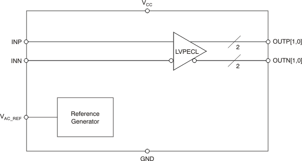
The CDCLVP1102 clock buffer distributes a single clock input (IN) to two pairs of differential LVPECL clock outputs (OUT0, OUT1) with minimum skew for clock distribution. The inputs can be LVPECL, LVDS, or LVCMOS/LVTTL.
The CDCLVP1102 is specifically designed for driving 50-Ω transmission lines. When driving the inputs in single-ended mode, the LVPECL bias voltage (VAC_REF) should be applied to the unused negative input pin. However, for high-speed performance up to 2 GHz, differential mode is strongly recommended.
The CDCLVP1102 is characterized for operation from –40°C to 85°C and is available in a QFN-16, 3-mm × 3-mm package.


